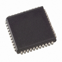
AT89LP6440-20JU Atmel, AT89LP6440-20JU Datasheet - Page 90

AT89LP6440-20JU
Manufacturer Part Number
AT89LP6440-20JU
Description
MCU 8051 64K FLASH ISP 44PLCC
Manufacturer
Atmel
Series
89LPr
Datasheet
1.AT89LP6440-20MU.pdf
(194 pages)
Specifications of AT89LP6440-20JU
Core Processor
8051
Core Size
8-Bit
Speed
20MHz
Connectivity
I²C, SPI, UART/USART
Peripherals
Brown-out Detect/Reset, POR, PWM, WDT
Number Of I /o
38
Program Memory Size
64KB (64K x 8)
Program Memory Type
FLASH
Eeprom Size
8K x 8
Ram Size
4.25K x 8
Voltage - Supply (vcc/vdd)
2.4 V ~ 3.6 V
Data Converters
A/D 8x10b
Oscillator Type
Internal
Operating Temperature
-40°C ~ 85°C
Package / Case
44-PLCC
Processor Series
AT89x
Core
8051
Data Bus Width
8 bit
Data Ram Size
8 KB
Interface Type
2-Wire, SPI
Maximum Clock Frequency
24 MHz
Number Of Programmable I/os
38
Number Of Timers
3
Operating Supply Voltage
2.7 V to 3.6 V
Maximum Operating Temperature
+ 85 C
Mounting Style
SMD/SMT
3rd Party Development Tools
PK51, CA51, A51, ULINK2
Development Tools By Supplier
AT89ISP
Minimum Operating Temperature
- 40 C
On-chip Adc
10 bit, 8 Channel
On-chip Dac
10 bit, 8 Channel
Lead Free Status / RoHS Status
Lead free / RoHS Compliant
Available stocks
Company
Part Number
Manufacturer
Quantity
Price
Company:
Part Number:
AT89LP6440-20JU
Manufacturer:
Atmel
Quantity:
103
- Current page: 90 of 194
- Download datasheet (6Mb)
Figure 16-2. Mode 0 Waveforms
Figure 16-3. UART Mode 0 TWI Emulation (SMOD1 = 1)
90
Write to SBUF
(SDA) RXD
(SCL) TXD
AT89LP6440 - Preliminary
SMOD1 = 0
SM2 = 0
SMOD1 = 1
SM2 = 0
SMOD1 = 0
SM2 = 1
SMOD1 = 1
SM2 = 1
SM2
P3.0
TI
RXD (RX)
RXD (RX)
RXD (RX)
RXD (RX)
RXD (TX)
RXD (TX)
RXD (TX)
RXD (TX)
Mode 0 may be used as a hardware accelerator for software emulation of serial interfaces such
as a half-duplex Serial Peripheral Interface (SPI) in mode (0,0) or (1,1) or a Two-Wire Interface
(TWI) in master mode. An example of Mode 0 emulating a TWI master device is shown in
16-3. In this example, the start, stop, and acknowledge are handled in software while the byte
transmission is done in hardware. Falling/rising edges on TXD are created by setting/clearing
SM2. Rising/falling edges on RXD are forced by setting/clearing the P3.0 register bit. SM2 and
P3.0 must be 1 while the byte is being transferred.
Mode 0 transfers data LSB first whereas SPI or TWI are generally MSB first. Emulation of these
interfaces may require bit reversal of the transferred data bytes. The following code example
reverses the bits in the accumulator:
TXD
TXD
TXD
TXD
EX:
REVRS: RLC
0
MOV
XCH
RRC
XCH
DJNZ R7, REVRS
1
0
0
0
0
0
0
0
0
R7, #8
A
A, R6
A
A, R6
2
1
1
1
1
1
1
1
1
3
2
2
2
2
2
2
2
2
; C << msb(ACC)
; msb(ACC) >> B
4
3
3
3
3
3
3
3
3
5
4
4
4
4
4
4
4
4
6
5
5
5
5
5
5
Sample ACK
5
5
7
6
6
6
6
6
6
6
6
ACK
7
7
7
7
7
7
7
7
3706A–MICRO–9/09
Figure
Related parts for AT89LP6440-20JU
Image
Part Number
Description
Manufacturer
Datasheet
Request
R

Part Number:
Description:
DEV KIT FOR AVR/AVR32
Manufacturer:
Atmel
Datasheet:

Part Number:
Description:
INTERVAL AND WIPE/WASH WIPER CONTROL IC WITH DELAY
Manufacturer:
ATMEL Corporation
Datasheet:

Part Number:
Description:
Low-Voltage Voice-Switched IC for Hands-Free Operation
Manufacturer:
ATMEL Corporation
Datasheet:

Part Number:
Description:
MONOLITHIC INTEGRATED FEATUREPHONE CIRCUIT
Manufacturer:
ATMEL Corporation
Datasheet:

Part Number:
Description:
AM-FM Receiver IC U4255BM-M
Manufacturer:
ATMEL Corporation
Datasheet:

Part Number:
Description:
Monolithic Integrated Feature Phone Circuit
Manufacturer:
ATMEL Corporation
Datasheet:

Part Number:
Description:
Multistandard Video-IF and Quasi Parallel Sound Processing
Manufacturer:
ATMEL Corporation
Datasheet:

Part Number:
Description:
High-performance EE PLD
Manufacturer:
ATMEL Corporation
Datasheet:

Part Number:
Description:
8-bit Flash Microcontroller
Manufacturer:
ATMEL Corporation
Datasheet:

Part Number:
Description:
2-Wire Serial EEPROM
Manufacturer:
ATMEL Corporation
Datasheet:


