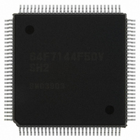
HD64F7144F50V Renesas Electronics America, HD64F7144F50V Datasheet - Page 381

HD64F7144F50V
Manufacturer Part Number
HD64F7144F50V
Description
IC SUPERH MCU FLASH 256K 112QFP
Manufacturer
Renesas Electronics America
Series
SuperH® SH7144r
Specifications of HD64F7144F50V
Core Processor
SH-2
Core Size
32-Bit
Speed
50MHz
Connectivity
EBI/EMI, I²C, SCI
Peripherals
DMA, POR, PWM, WDT
Number Of I /o
74
Program Memory Size
256KB (256K x 8)
Program Memory Type
FLASH
Ram Size
8K x 8
Voltage - Supply (vcc/vdd)
3 V ~ 3.6 V
Data Converters
A/D 8x10b
Oscillator Type
Internal
Operating Temperature
-20°C ~ 75°C
Package / Case
112-QFP
For Use With
HS0005KCU11H - EMULATOR E10A-USB H8S(X),SH2(A)EDK7145 - DEV EVALUATION KIT SH7145
Lead Free Status / RoHS Status
Lead free / RoHS Compliant
Eeprom Size
-
Available stocks
Company
Part Number
Manufacturer
Quantity
Price
Company:
Part Number:
HD64F7144F50V
Manufacturer:
RENESAS
Quantity:
450
Company:
Part Number:
HD64F7144F50V
Manufacturer:
Renesas Electronics America
Quantity:
10 000
Part Number:
HD64F7144F50V
Manufacturer:
RENESAS/瑞萨
Quantity:
20 000
- Current page: 381 of 932
- Download datasheet (6Mb)
11.
Multi-Function Timer Pulse Unit (MTU)
11.7.19 Output Level in Complementary PWM Mode and Reset-Synchronous PWM Mode
When channels 3 and 4 are in complementary PWM mode or reset-synchronous PWM mode, the
PWM waveform output level is set with the OLSP and OLSN bits in the timer output control
register (TOCR). In the case of complementary PWM mode or reset-synchronous PWM mode,
TIOR should be set to H'00.
11.7.20 Interrupts in Module Standby Mode
If module standby mode is entered when an interrupt has been requested, it will not be possible to
clear the CPU interrupt source or the DTC/DMAC activation source. Interrupts should therefore
be disabled before entering module standby mode.
11.7.21 Simultaneous Capture of TCNT_1 and TCNT_2 in Cascade Connection
When timer counters 1 and 2 (TCNT_1 and TCNT_2) are operated as a 32-bit counter in cascade
connection, the cascade counter value cannot be captured successfully even if input-capture input
is simultaneously done to TIOC1A and TIOC2A or to TIOC1B and TIOC2B. This is because the
input timing of TIOC1A and TIOC2A or of TIOC1B and TIOC2B may not be the same when
external input-capture signals to be input into TCNT_1 and TCNT_2 are taken in synchronization
with the internal clock. For example, TCNT_1 (the counter for upper 16 bits) does not capture the
count-up value by overflow from TCNT_2 (the counter for lower 16 bits) but captures the count
value before the count-up. In this case, the values of TCNT_1 = H'FFF1 and TCNT_2 = H'0000
should be transferred to TGRA_1 and TGRA_2 or to TGRB_1 and TGRB_2, but the values of
TCNT_1 = H'FFF0 and TCNT_2 = H'0000 are erroneously transferred.
11.7.22 Note on Buffer Operation Setting
When enabling buffer operation, clear to 0 bits TGIEC and TGIED (corresponding to TGRC and
TGRD, which are used as buffer registers) in the timer interrupt enable register (TIER).
Rev.4.00 Mar. 27, 2008 Page 335 of 882
REJ09B0108-0400
Related parts for HD64F7144F50V
Image
Part Number
Description
Manufacturer
Datasheet
Request
R

Part Number:
Description:
KIT STARTER FOR M16C/29
Manufacturer:
Renesas Electronics America
Datasheet:

Part Number:
Description:
KIT STARTER FOR R8C/2D
Manufacturer:
Renesas Electronics America
Datasheet:

Part Number:
Description:
R0K33062P STARTER KIT
Manufacturer:
Renesas Electronics America
Datasheet:

Part Number:
Description:
KIT STARTER FOR R8C/23 E8A
Manufacturer:
Renesas Electronics America
Datasheet:

Part Number:
Description:
KIT STARTER FOR R8C/25
Manufacturer:
Renesas Electronics America
Datasheet:

Part Number:
Description:
KIT STARTER H8S2456 SHARPE DSPLY
Manufacturer:
Renesas Electronics America
Datasheet:

Part Number:
Description:
KIT STARTER FOR R8C38C
Manufacturer:
Renesas Electronics America
Datasheet:

Part Number:
Description:
KIT STARTER FOR R8C35C
Manufacturer:
Renesas Electronics America
Datasheet:

Part Number:
Description:
KIT STARTER FOR R8CL3AC+LCD APPS
Manufacturer:
Renesas Electronics America
Datasheet:

Part Number:
Description:
KIT STARTER FOR RX610
Manufacturer:
Renesas Electronics America
Datasheet:

Part Number:
Description:
KIT STARTER FOR R32C/118
Manufacturer:
Renesas Electronics America
Datasheet:

Part Number:
Description:
KIT DEV RSK-R8C/26-29
Manufacturer:
Renesas Electronics America
Datasheet:

Part Number:
Description:
KIT STARTER FOR SH7124
Manufacturer:
Renesas Electronics America
Datasheet:

Part Number:
Description:
KIT STARTER FOR H8SX/1622
Manufacturer:
Renesas Electronics America
Datasheet:


