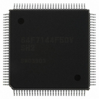
HD64F7144F50V Renesas Electronics America, HD64F7144F50V Datasheet - Page 514

HD64F7144F50V
Manufacturer Part Number
HD64F7144F50V
Description
IC SUPERH MCU FLASH 256K 112QFP
Manufacturer
Renesas Electronics America
Series
SuperH® SH7144r
Specifications of HD64F7144F50V
Core Processor
SH-2
Core Size
32-Bit
Speed
50MHz
Connectivity
EBI/EMI, I²C, SCI
Peripherals
DMA, POR, PWM, WDT
Number Of I /o
74
Program Memory Size
256KB (256K x 8)
Program Memory Type
FLASH
Ram Size
8K x 8
Voltage - Supply (vcc/vdd)
3 V ~ 3.6 V
Data Converters
A/D 8x10b
Oscillator Type
Internal
Operating Temperature
-20°C ~ 75°C
Package / Case
112-QFP
For Use With
HS0005KCU11H - EMULATOR E10A-USB H8S(X),SH2(A)EDK7145 - DEV EVALUATION KIT SH7145
Lead Free Status / RoHS Status
Lead free / RoHS Compliant
Eeprom Size
-
Available stocks
Company
Part Number
Manufacturer
Quantity
Price
Company:
Part Number:
HD64F7144F50V
Manufacturer:
RENESAS
Quantity:
450
Company:
Part Number:
HD64F7144F50V
Manufacturer:
Renesas Electronics America
Quantity:
10 000
Part Number:
HD64F7144F50V
Manufacturer:
RENESAS/瑞萨
Quantity:
20 000
- Current page: 514 of 932
- Download datasheet (6Mb)
14. I
14.1
• Selection of addressing or non-addressing format
• This I
• In the I
• Automatic creation of start and stop conditions in master mode of the I
• Selectable acknowledge output level during reception in the I
• Automatic loading of the acknowledge bit is available during transmission in the I
• A wait function is available in the I
• A wait function is available in the I
• Interrupt sources
• Sixteen variants of the internal clock are selectable in the master mode.
• Direct bus drive (SCL/SDA pin)
Rev.4.00 Mar. 27, 2008 Page 468 of 882
REJ09B0108-0400
I
Synchronous serial format: non-addressing format without an acknowledge bit, and with
master operation only
format.
After all data other than the acknowledge bit has been transferred, the system can be placed in
the wait state by setting SCL low. The wait state can be cancelled by clearing the interrupt flag
to 0.
After all data other than the acknowledge bit has been transferred, a request to enter the wait
state can be issued by setting SCL low. The request to enter the wait state is cleared when the
next transfer becomes possible.
Data transfer end (including when a transition to transmit mode is made in the I
when data in ICDR is transferred, or during a wait state)
Address match: when any slave address matches or the general call address is received in slave
receive mode of the I
contention)
Loss of arbitration
Start condition detection (in master mode)
Stop condition detection (in slave mode)
Pins SCL0 and SDA0 function as NMOS open-drain output.
2
C bus format: addressing format with an acknowledge bit, master and slave operation
2
C Bus Interface (IIC) Option
2
Features
C bus format complies with the I
2
C bus format, two slave addresses are specifiable for a single device.
2
C bus format (including address reception after loss in master
2
2
C bus format in the master mode.
C bus format.
2
C bus interface advocated by Phillips.
2
C bus format
2
C bus format
2
C bus format,
2
C bus
Related parts for HD64F7144F50V
Image
Part Number
Description
Manufacturer
Datasheet
Request
R

Part Number:
Description:
KIT STARTER FOR M16C/29
Manufacturer:
Renesas Electronics America
Datasheet:

Part Number:
Description:
KIT STARTER FOR R8C/2D
Manufacturer:
Renesas Electronics America
Datasheet:

Part Number:
Description:
R0K33062P STARTER KIT
Manufacturer:
Renesas Electronics America
Datasheet:

Part Number:
Description:
KIT STARTER FOR R8C/23 E8A
Manufacturer:
Renesas Electronics America
Datasheet:

Part Number:
Description:
KIT STARTER FOR R8C/25
Manufacturer:
Renesas Electronics America
Datasheet:

Part Number:
Description:
KIT STARTER H8S2456 SHARPE DSPLY
Manufacturer:
Renesas Electronics America
Datasheet:

Part Number:
Description:
KIT STARTER FOR R8C38C
Manufacturer:
Renesas Electronics America
Datasheet:

Part Number:
Description:
KIT STARTER FOR R8C35C
Manufacturer:
Renesas Electronics America
Datasheet:

Part Number:
Description:
KIT STARTER FOR R8CL3AC+LCD APPS
Manufacturer:
Renesas Electronics America
Datasheet:

Part Number:
Description:
KIT STARTER FOR RX610
Manufacturer:
Renesas Electronics America
Datasheet:

Part Number:
Description:
KIT STARTER FOR R32C/118
Manufacturer:
Renesas Electronics America
Datasheet:

Part Number:
Description:
KIT DEV RSK-R8C/26-29
Manufacturer:
Renesas Electronics America
Datasheet:

Part Number:
Description:
KIT STARTER FOR SH7124
Manufacturer:
Renesas Electronics America
Datasheet:

Part Number:
Description:
KIT STARTER FOR H8SX/1622
Manufacturer:
Renesas Electronics America
Datasheet:


