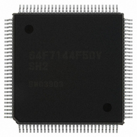
HD64F7144F50V Renesas Electronics America, HD64F7144F50V Datasheet - Page 575

HD64F7144F50V
Manufacturer Part Number
HD64F7144F50V
Description
IC SUPERH MCU FLASH 256K 112QFP
Manufacturer
Renesas Electronics America
Series
SuperH® SH7144r
Specifications of HD64F7144F50V
Core Processor
SH-2
Core Size
32-Bit
Speed
50MHz
Connectivity
EBI/EMI, I²C, SCI
Peripherals
DMA, POR, PWM, WDT
Number Of I /o
74
Program Memory Size
256KB (256K x 8)
Program Memory Type
FLASH
Ram Size
8K x 8
Voltage - Supply (vcc/vdd)
3 V ~ 3.6 V
Data Converters
A/D 8x10b
Oscillator Type
Internal
Operating Temperature
-20°C ~ 75°C
Package / Case
112-QFP
For Use With
HS0005KCU11H - EMULATOR E10A-USB H8S(X),SH2(A)EDK7145 - DEV EVALUATION KIT SH7145
Lead Free Status / RoHS Status
Lead free / RoHS Compliant
Eeprom Size
-
Available stocks
Company
Part Number
Manufacturer
Quantity
Price
Company:
Part Number:
HD64F7144F50V
Manufacturer:
RENESAS
Quantity:
450
Company:
Part Number:
HD64F7144F50V
Manufacturer:
Renesas Electronics America
Quantity:
10 000
Part Number:
HD64F7144F50V
Manufacturer:
RENESAS/瑞萨
Quantity:
20 000
- Current page: 575 of 932
- Download datasheet (6Mb)
4. The SCL and SDA inputs are sampled in synchronization with Pφ. Therefore, the AC timing
5. The SCL rising time t
Table 14.9 Tolerance of the SCL Rise Time (t
6. The rise and fall times of SCL and SDA are respectively prescribed as being 1000 ns or less
IICX
0
1
depends on the period of Pφ cycle t
timing specifications of the I
The I
a bit-by-bit basis. When the rise time t
level) of SCL exceeds the time determined by the input clock of the I
level period of SCL is extended. The time SCL takes to rise is determined by the pull-up
resistance and the load capacitance. Therefore, to operate at the specified transfer rate, set the
pull-up resistance and load capacitance so that each time is within the corresponding value
given in table 14.9.
and 300 ns or less by the I
bus interface of this LSI are described by t
effect of the rise and fall times, the I
maximum transfer rate. Table 14.10 shows the results of calculating the output timing for each
available operating frequency, by considering the worst-case rise and fall times. t
satisfy the specifications of the I
countermeasures against this problem:
A. Ensure that your program provides the required interval (approximately 1 μs) between
B. Select a slave device with an input timing that permits use with this output timing for
issuing of the stop condition and of the next start condition.
connection to the I
t
7.5 t
17.5
t
2
pcyc
C bus interface monitors SCL in the master mode, and communication is synchronized in
pcyc
pcyc
Standard
mode
High-speed
mode
Standard
mode
High-speed
mode
Sr
2
C bus.
is defined as being within 1,000 ns (300 ns in the high-speed mode).
I
specification
(Max.)
1000
300
1000
300
2
C bus
2
C bus specification. The output timing of SCL and SDA for the I
2
C bus interface are not satisfied.
2
C bus interface specifications. Take either of the following
pcyc
2
C bus interface specifications may not be satisfied at the
. When the Pφ frequency does not reach 5 MHz, the AC
Sr
Pφ=
10MHz
750
←
←
←
(the time required to reach V
pcyc
as shown in table 14.8. However, due to the
Sr
)
Pφ=
16MHz
468
←
←
←
Rev.4.00 Mar. 27, 2008 Page 529 of 882
Time [ns]
Pφ=
20MHz
375
←
875
←
14. I
2
C Bus Interface (IIC) Option
Pφ=
25MHz
300
←
700
←
IH
2
C bus interface, the high-
from an initially low
REJ09B0108-0400
Pφ=
33MHz
227
227
530
←
BUFO
does not
Pφ=
40MHz
188
188
438
←
2
C
Related parts for HD64F7144F50V
Image
Part Number
Description
Manufacturer
Datasheet
Request
R

Part Number:
Description:
KIT STARTER FOR M16C/29
Manufacturer:
Renesas Electronics America
Datasheet:

Part Number:
Description:
KIT STARTER FOR R8C/2D
Manufacturer:
Renesas Electronics America
Datasheet:

Part Number:
Description:
R0K33062P STARTER KIT
Manufacturer:
Renesas Electronics America
Datasheet:

Part Number:
Description:
KIT STARTER FOR R8C/23 E8A
Manufacturer:
Renesas Electronics America
Datasheet:

Part Number:
Description:
KIT STARTER FOR R8C/25
Manufacturer:
Renesas Electronics America
Datasheet:

Part Number:
Description:
KIT STARTER H8S2456 SHARPE DSPLY
Manufacturer:
Renesas Electronics America
Datasheet:

Part Number:
Description:
KIT STARTER FOR R8C38C
Manufacturer:
Renesas Electronics America
Datasheet:

Part Number:
Description:
KIT STARTER FOR R8C35C
Manufacturer:
Renesas Electronics America
Datasheet:

Part Number:
Description:
KIT STARTER FOR R8CL3AC+LCD APPS
Manufacturer:
Renesas Electronics America
Datasheet:

Part Number:
Description:
KIT STARTER FOR RX610
Manufacturer:
Renesas Electronics America
Datasheet:

Part Number:
Description:
KIT STARTER FOR R32C/118
Manufacturer:
Renesas Electronics America
Datasheet:

Part Number:
Description:
KIT DEV RSK-R8C/26-29
Manufacturer:
Renesas Electronics America
Datasheet:

Part Number:
Description:
KIT STARTER FOR SH7124
Manufacturer:
Renesas Electronics America
Datasheet:

Part Number:
Description:
KIT STARTER FOR H8SX/1622
Manufacturer:
Renesas Electronics America
Datasheet:


