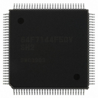
HD64F7144F50V Renesas Electronics America, HD64F7144F50V Datasheet - Page 820

HD64F7144F50V
Manufacturer Part Number
HD64F7144F50V
Description
IC SUPERH MCU FLASH 256K 112QFP
Manufacturer
Renesas Electronics America
Series
SuperH® SH7144r
Specifications of HD64F7144F50V
Core Processor
SH-2
Core Size
32-Bit
Speed
50MHz
Connectivity
EBI/EMI, I²C, SCI
Peripherals
DMA, POR, PWM, WDT
Number Of I /o
74
Program Memory Size
256KB (256K x 8)
Program Memory Type
FLASH
Ram Size
8K x 8
Voltage - Supply (vcc/vdd)
3 V ~ 3.6 V
Data Converters
A/D 8x10b
Oscillator Type
Internal
Operating Temperature
-20°C ~ 75°C
Package / Case
112-QFP
For Use With
HS0005KCU11H - EMULATOR E10A-USB H8S(X),SH2(A)EDK7145 - DEV EVALUATION KIT SH7145
Lead Free Status / RoHS Status
Lead free / RoHS Compliant
Eeprom Size
-
Available stocks
Company
Part Number
Manufacturer
Quantity
Price
Company:
Part Number:
HD64F7144F50V
Manufacturer:
RENESAS
Quantity:
450
Company:
Part Number:
HD64F7144F50V
Manufacturer:
Renesas Electronics America
Quantity:
10 000
Part Number:
HD64F7144F50V
Manufacturer:
RENESAS/瑞萨
Quantity:
20 000
- Current page: 820 of 932
- Download datasheet (6Mb)
26. Electrical Characteristics
26.3.3
Table 26.5 shows control signal timing.
Table 26.5 Control Signal Timing
Conditions: V
[Operating Precautions]
* The RES, MRES, NMI and IRQ7 to IRQ0 signals are asynchronous inputs, but when the setup
Rev.4.00 Mar. 27, 2008 Page 774 of 882
REJ09B0108-0400
Item
RES rise time, fall time
RES pulse width
RES setup time
MRES pulse width
MRES setup time
MD3 to MD0 setup time
NMI rise time, fall time
NMI setup time
NMI hold time
IRQ7 to IRQ0 setup time* (edge detection)
IRQ7 to IRQ0 setup time* (level detection)
IRQ7 to IRQ0 hold time
IRQOUT output delay time
Bus request setup time
Bus acknowledge delay time 1
Bus acknowledge delay time 2
Bus three-state delay time
times shown here are observed, the signals are considered to have been changed at clock rise
(RES, MRES) or fall (NMI and IRQ7 to IRQ0). If the setup times are not observed, the
recognition of these signals may be delayed until the next clock rise or fall.
Control Signal Timing
AV
(regular specifications), T
When programming or erasing flash memory, T
CC
ref
= PLLV
= 3.0 V to AV
CC
=3.3 V ± 0.3 V, AV
CC
, V
SS
a
= –40°C to +85°C (wide-range specifications),
= PLLV
Symbol
t
t
t
t
t
t
t
t
t
t
t
t
t
t
t
t
t
RESr
RESW
RESS
MRESW
MRESS
MDS
NMIr
NMIS
NMIH
IRQES
IRQLS
IRQEH
IRQOD
BRQS
BACKD1
BACKD2
BZD
CC
, t
SS
, t
= 3.3 V ± 0.3 V, AV
NMIf
RESf
= AV
SS
Min.
⎯
25
35
20
35
20
⎯
35
35
19
19
19
⎯
19
⎯
⎯
⎯
= 0 V, T
a
= –20°C to +75°C.
a
Max.
200
⎯
⎯
⎯
⎯
⎯
200
⎯
⎯
⎯
⎯
⎯
100
⎯
35
35
35
= –20°C to +75°C
CC
= V
Unit
ns
t
ns
t
ns
t
ns
ns
ns
ns
ns
ns
ns
ns
ns
ns
ns
CC
cyc
cyc
cyc
± 0.3 V,
Figure
Figure 26.5
Figure 26.6
Figure 26.7
Figure 26.8
Related parts for HD64F7144F50V
Image
Part Number
Description
Manufacturer
Datasheet
Request
R

Part Number:
Description:
KIT STARTER FOR M16C/29
Manufacturer:
Renesas Electronics America
Datasheet:

Part Number:
Description:
KIT STARTER FOR R8C/2D
Manufacturer:
Renesas Electronics America
Datasheet:

Part Number:
Description:
R0K33062P STARTER KIT
Manufacturer:
Renesas Electronics America
Datasheet:

Part Number:
Description:
KIT STARTER FOR R8C/23 E8A
Manufacturer:
Renesas Electronics America
Datasheet:

Part Number:
Description:
KIT STARTER FOR R8C/25
Manufacturer:
Renesas Electronics America
Datasheet:

Part Number:
Description:
KIT STARTER H8S2456 SHARPE DSPLY
Manufacturer:
Renesas Electronics America
Datasheet:

Part Number:
Description:
KIT STARTER FOR R8C38C
Manufacturer:
Renesas Electronics America
Datasheet:

Part Number:
Description:
KIT STARTER FOR R8C35C
Manufacturer:
Renesas Electronics America
Datasheet:

Part Number:
Description:
KIT STARTER FOR R8CL3AC+LCD APPS
Manufacturer:
Renesas Electronics America
Datasheet:

Part Number:
Description:
KIT STARTER FOR RX610
Manufacturer:
Renesas Electronics America
Datasheet:

Part Number:
Description:
KIT STARTER FOR R32C/118
Manufacturer:
Renesas Electronics America
Datasheet:

Part Number:
Description:
KIT DEV RSK-R8C/26-29
Manufacturer:
Renesas Electronics America
Datasheet:

Part Number:
Description:
KIT STARTER FOR SH7124
Manufacturer:
Renesas Electronics America
Datasheet:

Part Number:
Description:
KIT STARTER FOR H8SX/1622
Manufacturer:
Renesas Electronics America
Datasheet:


