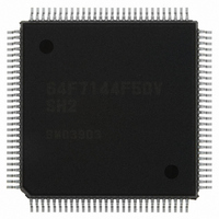
HD64F7144F50V Renesas Electronics America, HD64F7144F50V Datasheet - Page 557

HD64F7144F50V
Manufacturer Part Number
HD64F7144F50V
Description
IC SUPERH MCU FLASH 256K 112QFP
Manufacturer
Renesas Electronics America
Series
SuperH® SH7144r
Specifications of HD64F7144F50V
Core Processor
SH-2
Core Size
32-Bit
Speed
50MHz
Connectivity
EBI/EMI, I²C, SCI
Peripherals
DMA, POR, PWM, WDT
Number Of I /o
74
Program Memory Size
256KB (256K x 8)
Program Memory Type
FLASH
Ram Size
8K x 8
Voltage - Supply (vcc/vdd)
3 V ~ 3.6 V
Data Converters
A/D 8x10b
Oscillator Type
Internal
Operating Temperature
-20°C ~ 75°C
Package / Case
112-QFP
For Use With
HS0005KCU11H - EMULATOR E10A-USB H8S(X),SH2(A)EDK7145 - DEV EVALUATION KIT SH7145
Lead Free Status / RoHS Status
Lead free / RoHS Compliant
Eeprom Size
-
Available stocks
Company
Part Number
Manufacturer
Quantity
Price
Company:
Part Number:
HD64F7144F50V
Manufacturer:
RENESAS
Quantity:
450
Company:
Part Number:
HD64F7144F50V
Manufacturer:
Renesas Electronics America
Quantity:
10 000
Part Number:
HD64F7144F50V
Manufacturer:
RENESAS/瑞萨
Quantity:
20 000
- Current page: 557 of 932
- Download datasheet (6Mb)
The following description gives the procedures for and operations of receiving data in one byte
units by fixing SCL low for every data reception using the HNDS bit function.
1. Perform initialization according to the procedure described in section 14.4.2, Initialization.
2. Confirm that the ICDRF flag is 0. If the ICDRF flag is set to 1, read ICDR and then clear the
3. When the start condition output by the master device is detected, the BBSY flag in ICCR is set
4. When the slave address matches the address in the first frame following the start condition
5. The slave devise returns the data set in the ACKB bit as an acknowledgement at the 9th cycle
6. The IRIC flag is set to 1 at the 9th cycle of the clock. At this time, if the IEIC bit is set to 1, an
7. At the rising edge of the 9th cycle of the clock, the receive data is transferred from ICDRS to
8. Confirm that the STOP bit is cleared to 0, and then clear the IRIC flag to 0.
9. When the next frame is the final receive flame, clear the ACKB bit to 1.
10. After ICDR has been read, the ICDRF flag is cleared to 0 and the SCL bus line is released.
11. After the stop condition (when SCL is high, the SDA is changed from low to high) is detected,
12. Confirm that the STOP bit is set to 1, and then clear the IRIC flag to 0.
Set slave receive mode by clearing the MST and TRS bits to 0. Set the HNDS bit to 1 and the
ACKB bit to 0. To confirm the receive completion, clear the IRIC flag in ICCR to 0.
IRIC flag to 0.
to 1. The master device then outputs the 7-bit slave address and transmit/receive direction
(R/W) data in synchronization with the transmit clock pulses.
generation, the slave device operates as the slave devise specified by the master device. When
the 8th bit of data (R/W) is 0, the TRS bit remains 0 and slave receive operation is performed.
When the 8th bit of data (R/W) is 1, the TRS bit is set to 1 and slave transmit operation is
performed.
When addresses do not match, data receive operation is not performed until the next start
condition is detected.
of the receive frame of the clock.
interrupt request is generated for the CPU.
If the AASX bit is also set to 1, the IRTR flag is set to 1.
ICDRR and the ICDRF flag is set to 1. The slave device keeps SCL low from the falling edge
of the 9th cycle of the receive clock until data in ICDR is read.
This enables master device to transfer the next data.
Receive operation can be continued by repeating steps 5 to 10.
the BBSY flag is cleared to 0 and the STOP bit is set to 1. At this time, if the STOPIM bit is
cleared to 0, the IRIC flag is set to 1.
Rev.4.00 Mar. 27, 2008 Page 511 of 882
14. I
2
C Bus Interface (IIC) Option
REJ09B0108-0400
Related parts for HD64F7144F50V
Image
Part Number
Description
Manufacturer
Datasheet
Request
R

Part Number:
Description:
KIT STARTER FOR M16C/29
Manufacturer:
Renesas Electronics America
Datasheet:

Part Number:
Description:
KIT STARTER FOR R8C/2D
Manufacturer:
Renesas Electronics America
Datasheet:

Part Number:
Description:
R0K33062P STARTER KIT
Manufacturer:
Renesas Electronics America
Datasheet:

Part Number:
Description:
KIT STARTER FOR R8C/23 E8A
Manufacturer:
Renesas Electronics America
Datasheet:

Part Number:
Description:
KIT STARTER FOR R8C/25
Manufacturer:
Renesas Electronics America
Datasheet:

Part Number:
Description:
KIT STARTER H8S2456 SHARPE DSPLY
Manufacturer:
Renesas Electronics America
Datasheet:

Part Number:
Description:
KIT STARTER FOR R8C38C
Manufacturer:
Renesas Electronics America
Datasheet:

Part Number:
Description:
KIT STARTER FOR R8C35C
Manufacturer:
Renesas Electronics America
Datasheet:

Part Number:
Description:
KIT STARTER FOR R8CL3AC+LCD APPS
Manufacturer:
Renesas Electronics America
Datasheet:

Part Number:
Description:
KIT STARTER FOR RX610
Manufacturer:
Renesas Electronics America
Datasheet:

Part Number:
Description:
KIT STARTER FOR R32C/118
Manufacturer:
Renesas Electronics America
Datasheet:

Part Number:
Description:
KIT DEV RSK-R8C/26-29
Manufacturer:
Renesas Electronics America
Datasheet:

Part Number:
Description:
KIT STARTER FOR SH7124
Manufacturer:
Renesas Electronics America
Datasheet:

Part Number:
Description:
KIT STARTER FOR H8SX/1622
Manufacturer:
Renesas Electronics America
Datasheet:


