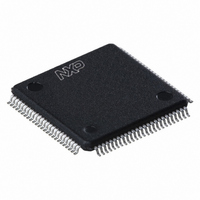
LPC2925FBD100,551 NXP Semiconductors, LPC2925FBD100,551 Datasheet - Page 14

LPC2925FBD100,551
Manufacturer Part Number
LPC2925FBD100,551
Description
IC ARM9 MCU FLASH 512KB 100-LQFP
Manufacturer
NXP Semiconductors
Series
LPC2900r
Datasheet
1.LPC2921FBD100551.pdf
(84 pages)
Specifications of LPC2925FBD100,551
Core Processor
ARM9
Core Size
32-Bit
Speed
125MHz
Connectivity
CAN, I²C, LIN, SPI, UART/USART, USB
Peripherals
DMA, POR, PWM, WDT
Number Of I /o
60
Program Memory Size
512KB (512K x 8)
Program Memory Type
FLASH
Eeprom Size
16K x 8
Ram Size
40K x 8
Voltage - Supply (vcc/vdd)
1.71 V ~ 3.6 V
Data Converters
A/D 16x8b
Oscillator Type
Internal
Operating Temperature
-40°C ~ 85°C
Package / Case
100-LQFP
Processor Series
LPC29
Core
ARM968E-S
3rd Party Development Tools
MDK-ARM, RL-ARM, ULINK2
Lead Free Status / RoHS Status
Lead free / RoHS Compliant
Other names
935287116551
Available stocks
Company
Part Number
Manufacturer
Quantity
Price
Company:
Part Number:
LPC2925FBD100,551
Manufacturer:
NXP Semiconductors
Quantity:
10 000
NXP Semiconductors
LPC2921_23_25_3
Product data sheet
Fig 4.
AHB MULTILAYER MATRIX
AHB TO APB BRIDGES
peripheral subsystem
SYSTEM CONTROL
USB REGISTERS
LPC2921/2923/2925 overview of clock areas
EVENT ROUTER
general subsytem
TIMER0/1/2/3
FLASH/SRAM
GPIO0/1/5
UART0/1
SPI0/1/2
GPDMA
WDT
CFID
VIC
CPU
6.7.2 Base clock and branch clock relationship
Two of the base clocks generated by the CGU0 are used as input into a second,
dedicated CGU (CGU1). The CGU1 uses its own PLL and fractional dividers to generate
the base clock for the USB controller and one base clock for an independent clock output.
Table 7
derived branch clocks. A short description is given of the hardware parts that are clocked
with the individual branch clocks. In relevant cases more detailed information can be
contains an overview of all the base blocks in the LPC2921/2923/2925 and their
CGU0
BASE_SYS_CLK
branch
clocks
All information provided in this document is subject to legal disclaimers.
Rev. 03 — 14 April 2010
BASE_ICLK0_CLK
BASE_ICLK1_CLK
BASE_IVNSS_CLK
BASE_MSCSS_CLK
BASE_PCR_CLK
ARM9 microcontroller with CAN, LIN, and USB
branch
branch
clocks
clock
branch
branch
clocks
clocks
LPC2921/2923/2925
modulation and sampling
networking subsystem
CGU1
power control subsystem
control subsystem
BASE_OUT_CLK
BASE_USB_CLK
ACCEPTANCE
TIMER0/1 MTMR
RESET/CLOCK
MANAGEMENT
GENERATION
PWM0/1/2/3
GLOBAL
CAN0/1
FILTER
LIN0/1
I
ADC1/2
2
POWER
C0/1
QEI
© NXP B.V. 2010. All rights reserved.
002aae238
CLOCK
OUT
USB
14 of 84


