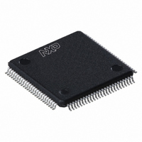
LPC2925FBD100,551 NXP Semiconductors, LPC2925FBD100,551 Datasheet - Page 26

LPC2925FBD100,551
Manufacturer Part Number
LPC2925FBD100,551
Description
IC ARM9 MCU FLASH 512KB 100-LQFP
Manufacturer
NXP Semiconductors
Series
LPC2900r
Datasheet
1.LPC2921FBD100551.pdf
(84 pages)
Specifications of LPC2925FBD100,551
Core Processor
ARM9
Core Size
32-Bit
Speed
125MHz
Connectivity
CAN, I²C, LIN, SPI, UART/USART, USB
Peripherals
DMA, POR, PWM, WDT
Number Of I /o
60
Program Memory Size
512KB (512K x 8)
Program Memory Type
FLASH
Eeprom Size
16K x 8
Ram Size
40K x 8
Voltage - Supply (vcc/vdd)
1.71 V ~ 3.6 V
Data Converters
A/D 16x8b
Oscillator Type
Internal
Operating Temperature
-40°C ~ 85°C
Package / Case
100-LQFP
Processor Series
LPC29
Core
ARM968E-S
3rd Party Development Tools
MDK-ARM, RL-ARM, ULINK2
Lead Free Status / RoHS Status
Lead free / RoHS Compliant
Other names
935287116551
Available stocks
Company
Part Number
Manufacturer
Quantity
Price
Company:
Part Number:
LPC2925FBD100,551
Manufacturer:
NXP Semiconductors
Quantity:
10 000
NXP Semiconductors
LPC2921_23_25_3
Product data sheet
6.12.4.1 Pin description
6.12.4.2 Clock description
6.12.5 Serial Peripheral Interface (SPI)
The UART is commonly used to implement a serial interface such as RS232. The
LPC2921/2923/2925 contains two industry-standard 550 UARTs with 16-byte transmit and
receive FIFOs, but they can also be put into 450 mode without FIFOs.
Remark: The LIN controller can be configured to provide two additional standard UART
interfaces (see
The UART pins are combined with other functions on the port pins of the
LPC2921/2923/2925.
Table 14.
The UART modules are clocked by two different clocks; CLK_SYS_PESS and
CLK_UARTx (x = 0 to 1), see
CLK_UARTx branch clock for power management. The frequency of all CLK_UARTx
clocks is identical since they are derived from the same base clock BASE_CLK_UART.
The register interface towards the system bus is clocked by CLK_SYS_PESS. The baud
generator is clocked by the CLK_UARTx.
The LPC2921/2923/2925 contains three Serial Peripheral Interface modules (SPIs) to
allow synchronous serial communication with slave or master peripherals.
The key features are:
Symbol
UARTx TXD
UARTx RXD
•
•
•
•
•
•
•
•
•
•
•
•
•
•
Register locations conform to 550 industry standard.
Receiver FIFO trigger points at 1 byte, 4 bytes, 8 bytes and 14 bytes.
Built-in baud rate generator.
Support for RS-485/9-bit mode allows both software address detection and automatic
address detection using 9-bit mode.
Master or slave operation.
Each SPI supports up to four slaves in sequential multi-slave operation.
Supports timer-triggered operation.
Programmable clock bit rate and prescale based on SPI source clock.
(BASE_SPI_CLK), independent of system clock.
Separate transmit and receive FIFO memory buffers; 16 bits wide, 32 locations deep.
Programmable choice of interface operation: Motorola SPI or Texas Instruments
Synchronous Serial Interfaces.
Programmable data-frame size from 4 bits to 16 bits.
Independent masking of transmit FIFO, receive FIFO and receive overrun interrupts.
Serial clock-rate master mode: fserial_clk ≤ f
Serial clock-rate slave mode: fserial_clk = f
UART pins
TXDx
RXDx
Pin name
Section
All information provided in this document is subject to legal disclaimers.
Table 14
Rev. 03 — 14 April 2010
6.13.2).
OUT
IN
Direction
Section
shows the UART pins (x runs from 0 to 1).
6.7.2. Note that each UART has its own
ARM9 microcontroller with CAN, LIN, and USB
UART channel x transmit data output
UART channel x receive data input
Description
clk(SPI)
LPC2921/2923/2925
clk(SPI)
/ 4.
/ 2.
© NXP B.V. 2010. All rights reserved.
26 of 84


