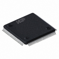
LPC2925FBD100,551 NXP Semiconductors, LPC2925FBD100,551 Datasheet - Page 55

LPC2925FBD100,551
Manufacturer Part Number
LPC2925FBD100,551
Description
IC ARM9 MCU FLASH 512KB 100-LQFP
Manufacturer
NXP Semiconductors
Series
LPC2900r
Datasheet
1.LPC2921FBD100551.pdf
(84 pages)
Specifications of LPC2925FBD100,551
Core Processor
ARM9
Core Size
32-Bit
Speed
125MHz
Connectivity
CAN, I²C, LIN, SPI, UART/USART, USB
Peripherals
DMA, POR, PWM, WDT
Number Of I /o
60
Program Memory Size
512KB (512K x 8)
Program Memory Type
FLASH
Eeprom Size
16K x 8
Ram Size
40K x 8
Voltage - Supply (vcc/vdd)
1.71 V ~ 3.6 V
Data Converters
A/D 16x8b
Oscillator Type
Internal
Operating Temperature
-40°C ~ 85°C
Package / Case
100-LQFP
Processor Series
LPC29
Core
ARM968E-S
3rd Party Development Tools
MDK-ARM, RL-ARM, ULINK2
Lead Free Status / RoHS Status
Lead free / RoHS Compliant
Other names
935287116551
Available stocks
Company
Part Number
Manufacturer
Quantity
Price
Company:
Part Number:
LPC2925FBD100,551
Manufacturer:
NXP Semiconductors
Quantity:
10 000
NXP Semiconductors
8. Static characteristics
Table 31.
V
measured with respect to ground; positive currents flow into the IC; unless otherwise specified.
LPC2921_23_25_3
Product data sheet
Symbol
Supplies
Core supply
V
I
I/O supply
V
I
Oscillator/PLL supply
V
I
Analog-to-digital converter supply
V
I
Input pins and I/O pins configured as input
V
V
V
V
DD(CORE)
DD(IO)
DD(OSC_PLL)
DDA(ADC3V3)
DD(CORE)
DD(CORE)
DD(IO)
DD(OSC_PLL)
DDA(ADC3V3)
I
IH
IL
hys
= V
Static characteristics
DD(OSC_PLL)
Parameter
core supply voltage
core supply current
input/output supply
voltage
I/O supply current
oscillator and PLL supply
voltage
oscillator and PLL supply
current
3.3 V ADC analog supply
voltage
3.3 V ADC analog supply
current
input voltage
HIGH-level input voltage
LOW-level input voltage
hysteresis voltage
; V
DD(IO)
= 2.7 V to 3.6 V; V
All information provided in this document is subject to legal disclaimers.
Device state after reset;
all port pins, RST, TRST,
Conditions
system clock at
125 MHz; T
executing code
while(1){} from flash.
all clocks off
Power-down mode
Normal mode
Power-down mode
Normal mode
Power-down mode
all port pins and V
applied;
see
port 0 pin 8 to pin 23
when ADC1/2 is used
all port pins and V
not applied
all other I/O pins, RST,
TRST, TDI, JTAGSEL,
TMS, TCK
TDI, JTAGSEL, TMS,
TCK
all port pins, RST, TRST,
TDI, JTAGSEL, TMS,
TCK
Section 7
Rev. 03 — 14 April 2010
DDA(ADC3V3)
amb
= 85 °C;
DD(IO)
DD(IO)
= 3.0 V to 3.6 V; T
ARM9 microcontroller with CAN, LIN, and USB
[3][4]
[2]
[4]
Min
1.71
-
-
2.7
1.71
-
3.0
-
−0.5
-
−0.5
−0.5
2.0
-
0.4
-
-
-
LPC2921/2923/2925
vj
=
−
40
°
C to +85
Typ
1.80
75
30
-
0.5
1.80
-
-
3.3
-
-
-
-
-
-
-
-
-
[1]
1.89
+ 5.5
Max
1.89
-
475
3.6
3.25
1
2
3.6
1.9
4
V
+3.6
V
-
0.8
-
°
C; all voltages are
VREFP
DD(IO)
© NXP B.V. 2010. All rights reserved.
55 of 84
Unit
V
mA
μA
V
μA
V
mA
μA
V
mA
μA
V
V
V
V
V
V


