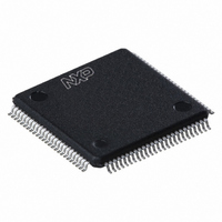
LPC2925FBD100,551 NXP Semiconductors, LPC2925FBD100,551 Datasheet - Page 27

LPC2925FBD100,551
Manufacturer Part Number
LPC2925FBD100,551
Description
IC ARM9 MCU FLASH 512KB 100-LQFP
Manufacturer
NXP Semiconductors
Series
LPC2900r
Datasheet
1.LPC2921FBD100551.pdf
(84 pages)
Specifications of LPC2925FBD100,551
Core Processor
ARM9
Core Size
32-Bit
Speed
125MHz
Connectivity
CAN, I²C, LIN, SPI, UART/USART, USB
Peripherals
DMA, POR, PWM, WDT
Number Of I /o
60
Program Memory Size
512KB (512K x 8)
Program Memory Type
FLASH
Eeprom Size
16K x 8
Ram Size
40K x 8
Voltage - Supply (vcc/vdd)
1.71 V ~ 3.6 V
Data Converters
A/D 16x8b
Oscillator Type
Internal
Operating Temperature
-40°C ~ 85°C
Package / Case
100-LQFP
Processor Series
LPC29
Core
ARM968E-S
3rd Party Development Tools
MDK-ARM, RL-ARM, ULINK2
Lead Free Status / RoHS Status
Lead free / RoHS Compliant
Other names
935287116551
Available stocks
Company
Part Number
Manufacturer
Quantity
Price
Company:
Part Number:
LPC2925FBD100,551
Manufacturer:
NXP Semiconductors
Quantity:
10 000
NXP Semiconductors
LPC2921_23_25_3
Product data sheet
6.12.5.1 Functional description
6.12.5.2 Pin description
The SPI module can operate in:
The SPI module is a master or slave interface for synchronous serial communication with
peripheral devices that have either Motorola SPI or Texas Instruments Synchronous
Serial Interfaces.
The SPI module performs serial-to-parallel conversion on data received from a peripheral
device. The transmit and receive paths are buffered with FIFO memories
(16 bits wide × 32 words deep). Serial data is transmitted on pins SDOx and received on
pins SDIx.
The SPI module includes a programmable bit-rate clock divider and prescaler to generate
the SPI serial clock from the input clock CLK_SPIx.
The SPI module’s operating mode, frame format, and word size are programmed through
the SLVn_SETTINGS registers.
A single combined interrupt request SPI_INTREQ output is asserted if any of the
interrupts are asserted and unmasked.
Depending on the operating mode selected, the SPI SCS outputs operate as an
active-HIGH frame synchronization output for Texas Instruments synchronous serial
frame format or an active-LOW chip select for SPI.
Each data frame is between four and 16 bits long, depending on the size of words
programmed, and is transmitted starting with the MSB.
The SPI pins are combined with other functions on the port pins of the
LPC2921/2923/2925, see
y runs from 0 to 3).
Table 15.
[1]
[2]
Symbol
SPIx SCSy
SPIx SCK
SPIx SDI
SPIx SDO
•
•
•
Internal loopback test mode.
Master mode:
– Normal transmission mode
– Sequential slave mode
Slave mode
Direction of SPIx SCS and SPIx SCK pins depends on master or slave mode. These pins are output in
master mode, input in slave mode.
In slave mode there is only one chip select input pin, SPIx SCS0. The other chip selects have no function in
slave mode.
SPI pins
SCSx[y]
SCKx
SDIx
SDOx
Pin name
All information provided in this document is subject to legal disclaimers.
Rev. 03 — 14 April 2010
Section
IN/OUT
IN
OUT
Direction
IN/OUT
6.11.3.
ARM9 microcontroller with CAN, LIN, and USB
SPIx data input
SPIx data output
Description
SPIx chip select
SPIx clock
Table 15
LPC2921/2923/2925
shows the SPI pins (x runs from 0 to 2;
[1]
[1][2]
© NXP B.V. 2010. All rights reserved.
27 of 84


