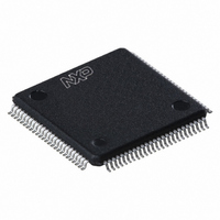
LPC2925FBD100,551 NXP Semiconductors, LPC2925FBD100,551 Datasheet - Page 2

LPC2925FBD100,551
Manufacturer Part Number
LPC2925FBD100,551
Description
IC ARM9 MCU FLASH 512KB 100-LQFP
Manufacturer
NXP Semiconductors
Series
LPC2900r
Datasheet
1.LPC2921FBD100551.pdf
(84 pages)
Specifications of LPC2925FBD100,551
Core Processor
ARM9
Core Size
32-Bit
Speed
125MHz
Connectivity
CAN, I²C, LIN, SPI, UART/USART, USB
Peripherals
DMA, POR, PWM, WDT
Number Of I /o
60
Program Memory Size
512KB (512K x 8)
Program Memory Type
FLASH
Eeprom Size
16K x 8
Ram Size
40K x 8
Voltage - Supply (vcc/vdd)
1.71 V ~ 3.6 V
Data Converters
A/D 16x8b
Oscillator Type
Internal
Operating Temperature
-40°C ~ 85°C
Package / Case
100-LQFP
Processor Series
LPC29
Core
ARM968E-S
3rd Party Development Tools
MDK-ARM, RL-ARM, ULINK2
Lead Free Status / RoHS Status
Lead free / RoHS Compliant
Other names
935287116551
Available stocks
Company
Part Number
Manufacturer
Quantity
Price
Company:
Part Number:
LPC2925FBD100,551
Manufacturer:
NXP Semiconductors
Quantity:
10 000
NXP Semiconductors
LPC2921_23_25_3
Product data sheet
Other peripherals:
Up to 60 general-purpose I/O pins with programmable pull-up, pull-down, or bus
keeper.
Vectored Interrupt Controller (VIC) with 16 priority levels.
Up to 16 level-sensitive external interrupt pins, including USB, CAN and LIN wake-up
features.
Configurable clock out pin for driving external system clocks.
Processor wake-up from power-down via external interrupt pins and CAN or LIN
activity.
Flexible Reset Generator Unit (RGU) able to control resets of individual modules.
Flexible Clock-Generation Unit (CGU) able to control clock frequency of individual
modules:
Second, dedicated CGU with its own PLL generates the USB clock and a configurable
clock output.
Highly configurable system Power Management Unit (PMU):
Standard ARM test and debug interface with real-time in-circuit emulator.
Boundary-scan test supported.
ETM/ETB debug functions with 8 kB of dedicated SRAM also accessible for
application code and data storage.
Dual power supply:
100-pin LQFP package.
−40 °C to +85 °C ambient operating temperature range.
Two 10-bit ADCs, 8-channels each, with 3.3 V measurement range provide 8
analog inputs each with conversion times as low as 2.44 μs per channel. Each
channel provides a compare function to minimize interrupts.
Multiple trigger-start option for all ADCs: timer, PWM, other ADC and external
signal input.
Four 32-bit timers each containing four capture-and-compare registers linked to
I/Os.
Four six-channel PWMs (Pulse Width Modulators) with capture and trap
functionality.
Two dedicated 32-bit timers to schedule and synchronize PWM and ADC.
Quadrature encoder interface that can monitor one external quadrature encoder.
32-bit watchdog with timer change protection, running on safe clock.
On-chip very low-power ring oscillator; fixed frequency of 0.4 MHz; always on to
provide a Safe_Clock source for system monitoring.
On-chip crystal oscillator with a recommended operating range from 10 MHz to
25 MHz. PLL input range 10 MHz to 25 MHz.
On-chip PLL allows CPU operation up to a maximum CPU rate of 125 MHz.
Generation of up to 11 base clocks.
Seven fractional dividers.
clock control of individual modules.
allows minimization of system operating power consumption in any configuration.
CPU operating voltage: 1.8 V ± 5 %.
I/O operating voltage: 2.7 V to 3.6 V; inputs tolerant up to 5.5 V.
All information provided in this document is subject to legal disclaimers.
Rev. 03 — 14 April 2010
ARM9 microcontroller with CAN, LIN, and USB
LPC2921/2923/2925
© NXP B.V. 2010. All rights reserved.
2 of 84


