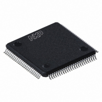
LPC2925FBD100,551 NXP Semiconductors, LPC2925FBD100,551 Datasheet - Page 35

LPC2925FBD100,551
Manufacturer Part Number
LPC2925FBD100,551
Description
IC ARM9 MCU FLASH 512KB 100-LQFP
Manufacturer
NXP Semiconductors
Series
LPC2900r
Datasheet
1.LPC2921FBD100551.pdf
(84 pages)
Specifications of LPC2925FBD100,551
Core Processor
ARM9
Core Size
32-Bit
Speed
125MHz
Connectivity
CAN, I²C, LIN, SPI, UART/USART, USB
Peripherals
DMA, POR, PWM, WDT
Number Of I /o
60
Program Memory Size
512KB (512K x 8)
Program Memory Type
FLASH
Eeprom Size
16K x 8
Ram Size
40K x 8
Voltage - Supply (vcc/vdd)
1.71 V ~ 3.6 V
Data Converters
A/D 16x8b
Oscillator Type
Internal
Operating Temperature
-40°C ~ 85°C
Package / Case
100-LQFP
Processor Series
LPC29
Core
ARM968E-S
3rd Party Development Tools
MDK-ARM, RL-ARM, ULINK2
Lead Free Status / RoHS Status
Lead free / RoHS Compliant
Other names
935287116551
Available stocks
Company
Part Number
Manufacturer
Quantity
Price
Company:
Part Number:
LPC2925FBD100,551
Manufacturer:
NXP Semiconductors
Quantity:
10 000
NXP Semiconductors
LPC2921_23_25_3
Product data sheet
Fig 6.
APB system bus
ADC block diagram
IRQ compare
6.14.4.2 Pin description
IRQ scan
A mechanism is provided to modify configuration of the ADC and control the moment at
which the updated configuration is transferred to the ADC domain.
The ADC clock is limited to 4.5 MHz maximum frequency and should always be lower
than or equal to the system clock frequency. To meet this constraint or to select the
desired lower sampling frequency, the clock generation unit provides a programmable
fractional system-clock divider dedicated to the ADC clock. Conversion rate is determined
by the ADC clock frequency divided by the number of resolution bits plus one. Accessing
ADC registers requires an enabled ADC clock, which is controllable via the clock
generation unit, see
Each ADC has four start inputs. Note that start 0 and start 2 are captured in the system
clock domain while start 1 and start 3 are captured in the ADC domain. The start inputs
are connected at MSCSS level, see
The two ADC modules in the MSCSS have the pins described below. The ADCx input
pins are combined with other functions on the port pins of the LPC2921/2923/2925. The
VREFN and VREFP pins are common for both ADCs.
Table 20.
Remark: Note that the ADC1 and ADC2 accept an input voltage up to of 3.6 V (see
Table
(BASE_MSCSS_CLK)
Symbol
ADC1/2 IN[7:0]
ADC2_EXT_START
VREFN
VREFP
V
DDA(ADC3V3)
start 0
ADC
REGISTERS
APB clock
31) on the ADC1/2 IN pins. If the ADC is not used, the pins are 5 V tolerant.
ADC
start 2
ADC
Analog to digital converter pins
SYSTEM DOMAIN
configuration data
conversion data
All information provided in this document is subject to legal disclaimers.
update
IRQ
Section
Pin name
IN1/2[7:0]
CAP1[2]
VREFN
VREFP
V
DDA(ADC3V3)
Rev. 03 — 14 April 2010
(BASE_ADC_CLK)
6.15.2.
start 1
(up to 4.5 MHz)
ADC
ADC clock
CONTROL
ADC
Direction
IN
IN
IN
IN
IN
Section 6.14
start 3
ADC
ARM9 microcontroller with CAN, LIN, and USB
sync_out
Description
analog input for 3.3 V ADC1/2, channel 7 to
channel 0
ADC external start-trigger input
ADC LOW reference level
ADC HIGH reference level
ADC1 and ADC2 3.3 V supply
ADC DOMAIN
LPC2921/2923/2925
for details.
ADC1
ADC2
3.3 V
3.3 V
Table 20
ANALOG
ANALOG
3.3 V IN
3.3 V IN
MUX
MUX
shows the ADC pins.
© NXP B.V. 2010. All rights reserved.
ADC1 IN[7:0]
ADC2 IN[7:0]
002aad960
35 of 84


