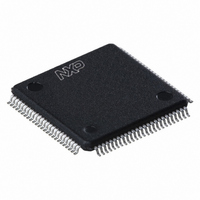
LPC2925FBD100,551 NXP Semiconductors, LPC2925FBD100,551 Datasheet - Page 19

LPC2925FBD100,551
Manufacturer Part Number
LPC2925FBD100,551
Description
IC ARM9 MCU FLASH 512KB 100-LQFP
Manufacturer
NXP Semiconductors
Series
LPC2900r
Datasheet
1.LPC2921FBD100551.pdf
(84 pages)
Specifications of LPC2925FBD100,551
Core Processor
ARM9
Core Size
32-Bit
Speed
125MHz
Connectivity
CAN, I²C, LIN, SPI, UART/USART, USB
Peripherals
DMA, POR, PWM, WDT
Number Of I /o
60
Program Memory Size
512KB (512K x 8)
Program Memory Type
FLASH
Eeprom Size
16K x 8
Ram Size
40K x 8
Voltage - Supply (vcc/vdd)
1.71 V ~ 3.6 V
Data Converters
A/D 16x8b
Oscillator Type
Internal
Operating Temperature
-40°C ~ 85°C
Package / Case
100-LQFP
Processor Series
LPC29
Core
ARM968E-S
3rd Party Development Tools
MDK-ARM, RL-ARM, ULINK2
Lead Free Status / RoHS Status
Lead free / RoHS Compliant
Other names
935287116551
Available stocks
Company
Part Number
Manufacturer
Quantity
Price
Company:
Part Number:
LPC2925FBD100,551
Manufacturer:
NXP Semiconductors
Quantity:
10 000
NXP Semiconductors
LPC2921_23_25_3
Product data sheet
6.8.3 Flash bridge wait-states
6.8.4 Pin description
6.8.5 Clock description
Table 10.
The index sector is a special sector in which the JTAG access protection and sector
security are located. The address space becomes visible by setting the FS_ISS bit and
overlaps the regular flash sector’s address space.
Note that the index sector, once programmed, cannot be erased. Any flash operation must
be executed out of SRAM (internal or external).
To eliminate the delay associated with synchronizing flash-read data, a predefined
number of wait-states must be programmed. These depend on flash memory response
time and system clock period. The minimum wait-states value can be calculated with the
following formulas:
Synchronous reading:
Asynchronous reading:
Remark: If the programmed number of wait-states is more than three, flash-data reading
cannot be performed at full speed (i.e. with zero wait-states at the AHB bus) if speculative
reading is active.
The flash memory controller has no external pins. However, the flash can be programmed
via the JTAG pins, see
The flash memory controller is clocked by CLK_SYS_FMC, see
WST
WST
Flash memory
sector number
16
17
18
0
1
2
3
4
5
6
>
>
t
----------------- -
t
--------------------- -
t
t
acc clk
acc addr
t
tclk sys
tclk sys
(
(
Flash sector overview
(
(
)
)
)
–
)
All information provided in this document is subject to legal disclaimers.
–
Sector size (kB)
8
8
8
64
64
64
64
64
64
64
1
1
Section
Rev. 03 — 14 April 2010
6.6.3.
…continued
Flash memory
address
0x2000 A000
0x2000 C000
0x2000 E000
0x2001 0000
0x2002 0000
0x2003 0000
0x2004 0000
0x2005 0000
0x2006 0000
0x2007 0000
ARM9 microcontroller with CAN, LIN, and USB
LPC2921/2923/2925
LPC2921
yes
yes
yes
yes
no
no
no
no
no
no
Section
LPC2923 LPC2925
yes
yes
yes
yes
yes
yes
no
no
no
no
© NXP B.V. 2010. All rights reserved.
6.7.2.
yes
yes
yes
yes
yes
yes
yes
yes
yes
yes
19 of 84
(1)
(2)


