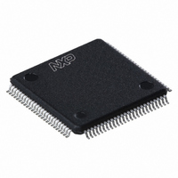
LPC2925FBD100,551 NXP Semiconductors, LPC2925FBD100,551 Datasheet - Page 57

LPC2925FBD100,551
Manufacturer Part Number
LPC2925FBD100,551
Description
IC ARM9 MCU FLASH 512KB 100-LQFP
Manufacturer
NXP Semiconductors
Series
LPC2900r
Datasheet
1.LPC2921FBD100551.pdf
(84 pages)
Specifications of LPC2925FBD100,551
Core Processor
ARM9
Core Size
32-Bit
Speed
125MHz
Connectivity
CAN, I²C, LIN, SPI, UART/USART, USB
Peripherals
DMA, POR, PWM, WDT
Number Of I /o
60
Program Memory Size
512KB (512K x 8)
Program Memory Type
FLASH
Eeprom Size
16K x 8
Ram Size
40K x 8
Voltage - Supply (vcc/vdd)
1.71 V ~ 3.6 V
Data Converters
A/D 16x8b
Oscillator Type
Internal
Operating Temperature
-40°C ~ 85°C
Package / Case
100-LQFP
Processor Series
LPC29
Core
ARM968E-S
3rd Party Development Tools
MDK-ARM, RL-ARM, ULINK2
Lead Free Status / RoHS Status
Lead free / RoHS Compliant
Other names
935287116551
Available stocks
Company
Part Number
Manufacturer
Quantity
Price
Company:
Part Number:
LPC2925FBD100,551
Manufacturer:
NXP Semiconductors
Quantity:
10 000
NXP Semiconductors
Table 31.
V
measured with respect to ground; positive currents flow into the IC; unless otherwise specified.
[1]
[2]
[3]
[4]
[5]
[6]
[7]
[8]
LPC2921_23_25_3
Product data sheet
Symbol
I
Oscillator
V
R
C
Power-up reset
V
V
V
OLS
DD(CORE)
XIN_OSC
trip(high)
trip(low)
trip(dif)
s(xtal)
i
All parameters are guaranteed over the virtual junction temperature range by design. Pre-testing is performed at T
level. Cased products are tested at T
the specified temperature and power-supply voltage range.
Leakage current is exponential to temperature; worst-case value is at 85 °C T
Not 5 V-tolerant when pull-up is on.
For I/O Port 0, the maximum input voltage is defined by V
For Port 0, pin 0 to pin 15 add maximum 1.5 pF for input capacitance to ADC. For Port 0, pin 16 to pin 31 add maximum 1.0 pF for input
capacitance to ADC.
C
This parameter is not part of production testing or final testing, hence only a typical value is stated. Maximum and minimum values are
based on simulation results.
The power-up reset has a time filter: V
V
trip(low)
xtal
is crystal load capacitance and C
= V
for 11 μs before internal reset is asserted.
Static characteristics
DD(OSC_PLL)
Parameter
LOW-level short-circuit
output current
voltage on pin XIN_OSC
crystal series resistance
input capacitance
high trip level voltage
low trip level voltage
difference between high
and low trip level voltage
; V
DD(IO)
= 2.7 V to 3.6 V; V
…continued
amb
ext
DD(CORE)
= 25 °C (final testing). Both pre-testing and final testing use correlated test conditions to cover
are the two external load capacitors.
All information provided in this document is subject to legal disclaimers.
Conditions
drive high; pad
connected to V
f
f
of XIN_OSC
osc
osc
C
C
C
C
C
C
must be above V
= 10 MHz to 15 MHz
xtal
ext
xtal
ext
= 15 MHz to 20 MHz
xtal
ext
= 18 pF
= 39 pF
= 18 pF
= 10 pF;
= 20 pF;
= 10 pF;
Rev. 03 — 14 April 2010
DDA(ADC3V3)
I(ADC)
DD(IO)
.
trip(high)
= 3.0 V to 3.6 V; T
for 2 μs before reset is de-asserted; V
ARM9 microcontroller with CAN, LIN, and USB
[6]
[6]
[7]
[8]
[8]
[8]
vj
. All clocks off. Analog modules and flash powered down.
Min
-
0
-
-
-
-
1.1
1.0
50
LPC2921/2923/2925
vj
=
−
40
°
C to +85
Typ
-
-
-
-
-
-
1.4
1.3
120
[1]
1.8
Max
95.1
160
60
80
2
1.6
1.5
180
°
DD(CORE)
C; all voltages are
© NXP B.V. 2010. All rights reserved.
amb
= 85 °C on wafer
must be below
57 of 84
Unit
mA
V
Ω
Ω
Ω
pF
V
V
mV


