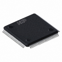
LPC2925FBD100,551 NXP Semiconductors, LPC2925FBD100,551 Datasheet - Page 47

LPC2925FBD100,551
Manufacturer Part Number
LPC2925FBD100,551
Description
IC ARM9 MCU FLASH 512KB 100-LQFP
Manufacturer
NXP Semiconductors
Series
LPC2900r
Datasheet
1.LPC2921FBD100551.pdf
(84 pages)
Specifications of LPC2925FBD100,551
Core Processor
ARM9
Core Size
32-Bit
Speed
125MHz
Connectivity
CAN, I²C, LIN, SPI, UART/USART, USB
Peripherals
DMA, POR, PWM, WDT
Number Of I /o
60
Program Memory Size
512KB (512K x 8)
Program Memory Type
FLASH
Eeprom Size
16K x 8
Ram Size
40K x 8
Voltage - Supply (vcc/vdd)
1.71 V ~ 3.6 V
Data Converters
A/D 16x8b
Oscillator Type
Internal
Operating Temperature
-40°C ~ 85°C
Package / Case
100-LQFP
Processor Series
LPC29
Core
ARM968E-S
3rd Party Development Tools
MDK-ARM, RL-ARM, ULINK2
Lead Free Status / RoHS Status
Lead free / RoHS Compliant
Other names
935287116551
Available stocks
Company
Part Number
Manufacturer
Quantity
Price
Company:
Part Number:
LPC2925FBD100,551
Manufacturer:
NXP Semiconductors
Quantity:
10 000
NXP Semiconductors
LPC2921_23_25_3
Product data sheet
Fig 12. Block diagram of the CGU1
BASE_ICLK0_CLK
BASE_ICLK1_CLK
6.15.3.1 Pin description
6.15.3 Clock generation for USB (CGU1)
6.15.4 Reset Generation Unit (RGU)
The CGU1 block is functionally identical to the CGU0 block and generates the clock for
the USB interface and a dedicated output clock. The CGU1 block uses its own PLL and
fractional divider. The PLLs used in CGU0 and CGU1 are identical (see
The clock input to the CGU1 PLL is provided by one of two base clocks generated in the
CGU0: BASE_ICLK0_CLK or BASE_ICLK1_CLK. The base clock not used for the PLL
can be configured to drive the output clock directly.
The CGU1 module in the LPC2921/2923/2925 has the pins listed in
Table 26.
The RGU controls all internal resets.
The key features of the Reset Generation Unit (RGU) are:
Symbol
CLK_OUT
•
•
•
Reset controlled individually per subsystem
Automatic reset stretching and release
Monitor function to trace resets back to source
CLOCK GENERATION UNIT
PLL
CGU1 pins
(CGU1)
clkout
clkout120
clkout240
All information provided in this document is subject to legal disclaimers.
Direction
OUT
Rev. 03 — 14 April 2010
AHB TO DTL BRIDGE
FDIV0
Description
clock output
ARM9 microcontroller with CAN, LIN, and USB
LPC2921/2923/2925
OUT 0
OUT 2
Table 25
© NXP B.V. 2010. All rights reserved.
Section
BASE_USB_CLK
BASE_OUT_CLK
002aae250
below.
6.15.2.2).
47 of 84


