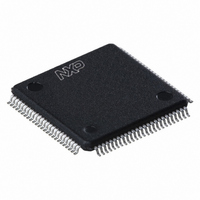
LPC2925FBD100,551 NXP Semiconductors, LPC2925FBD100,551 Datasheet - Page 29

LPC2925FBD100,551
Manufacturer Part Number
LPC2925FBD100,551
Description
IC ARM9 MCU FLASH 512KB 100-LQFP
Manufacturer
NXP Semiconductors
Series
LPC2900r
Datasheet
1.LPC2921FBD100551.pdf
(84 pages)
Specifications of LPC2925FBD100,551
Core Processor
ARM9
Core Size
32-Bit
Speed
125MHz
Connectivity
CAN, I²C, LIN, SPI, UART/USART, USB
Peripherals
DMA, POR, PWM, WDT
Number Of I /o
60
Program Memory Size
512KB (512K x 8)
Program Memory Type
FLASH
Eeprom Size
16K x 8
Ram Size
40K x 8
Voltage - Supply (vcc/vdd)
1.71 V ~ 3.6 V
Data Converters
A/D 16x8b
Oscillator Type
Internal
Operating Temperature
-40°C ~ 85°C
Package / Case
100-LQFP
Processor Series
LPC29
Core
ARM968E-S
3rd Party Development Tools
MDK-ARM, RL-ARM, ULINK2
Lead Free Status / RoHS Status
Lead free / RoHS Compliant
Other names
935287116551
Available stocks
Company
Part Number
Manufacturer
Quantity
Price
Company:
Part Number:
LPC2925FBD100,551
Manufacturer:
NXP Semiconductors
Quantity:
10 000
NXP Semiconductors
LPC2921_23_25_3
Product data sheet
6.12.6.3 Clock description
6.13.1.1 Global acceptance filter
6.13.1.2 Pin description
6.13.1 CAN gateway
6.13 Networking subsystem
The GPIO modules are clocked by several clocks, all of which are derived from
BASE_SYS_CLK; CLK_SYS_PESS and CLK_SYS_GPIOx (x = 0, 1, 5), see
Section
power management. The frequency of all clocks CLK_SYS_GPIOx is identical to
CLK_SYS_PESS since they are derived from the same base clock BASE_SYS_CLK.
Controller Area Network (CAN) is the definition of a high-performance communication
protocol for serial data communication. The two CAN controllers in the
LPC2921/2923/2925 provide a full implementation of the CAN protocol according to the
CAN specification version 2.0B. The gateway concept is fully scalable with the number of
CAN controllers, and always operates together with a separate powerful and flexible
hardware acceptance filter.
The key features are:
The global acceptance filter provides look-up of received identifiers - called acceptance
filtering in CAN terminology - for all the CAN controllers. It includes a CAN ID look-up table
memory, in which software maintains one to five sections of identifiers. The CAN ID
look-up table memory is 2 kB large (512 words, each of 32 bits). It can contain up to 1024
standard frame identifiers or 512 extended frame identifiers or a mixture of both types. It is
also possible to define identifier groups for standard and extended message formats.
The two CAN controllers in the LPC2921/2923/2925 have the pins listed below. The CAN
pins are combined with other functions on the port pins of the LPC2921/2923/2925.
Table 17
Table 17.
Symbol
CANx TXD
CANx RXD
•
•
•
•
•
•
•
•
Supports 11-bit as well as 29-bit identifiers.
Double receive buffer and triple transmit buffer.
Programmable error-warning limit and error counters with read/write access.
Arbitration-lost capture and error-code capture with detailed bit position.
Single-shot transmission (i.e. no re-transmission).
Listen-only mode (no acknowledge; no active error flags).
Reception of ‘own’ messages (self-reception request).
FullCAN mode for message reception.
6.7.2. Note that each GPIO has its own CLK__SYS_GPIOx branch clock for
shows the CAN pins (x runs from 0 to 1).
CAN pins
Pin name
TXDC0/1
RXDC0/1
All information provided in this document is subject to legal disclaimers.
Rev. 03 — 14 April 2010
IN
Direction
OUT
ARM9 microcontroller with CAN, LIN, and USB
CAN channel x transmit data output
CAN channel x receive data input
Description
LPC2921/2923/2925
© NXP B.V. 2010. All rights reserved.
29 of 84


