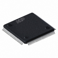
LPC2925FBD100,551 NXP Semiconductors, LPC2925FBD100,551 Datasheet - Page 46

LPC2925FBD100,551
Manufacturer Part Number
LPC2925FBD100,551
Description
IC ARM9 MCU FLASH 512KB 100-LQFP
Manufacturer
NXP Semiconductors
Series
LPC2900r
Datasheet
1.LPC2921FBD100551.pdf
(84 pages)
Specifications of LPC2925FBD100,551
Core Processor
ARM9
Core Size
32-Bit
Speed
125MHz
Connectivity
CAN, I²C, LIN, SPI, UART/USART, USB
Peripherals
DMA, POR, PWM, WDT
Number Of I /o
60
Program Memory Size
512KB (512K x 8)
Program Memory Type
FLASH
Eeprom Size
16K x 8
Ram Size
40K x 8
Voltage - Supply (vcc/vdd)
1.71 V ~ 3.6 V
Data Converters
A/D 16x8b
Oscillator Type
Internal
Operating Temperature
-40°C ~ 85°C
Package / Case
100-LQFP
Processor Series
LPC29
Core
ARM968E-S
3rd Party Development Tools
MDK-ARM, RL-ARM, ULINK2
Lead Free Status / RoHS Status
Lead free / RoHS Compliant
Other names
935287116551
Available stocks
Company
Part Number
Manufacturer
Quantity
Price
Company:
Part Number:
LPC2925FBD100,551
Manufacturer:
NXP Semiconductors
Quantity:
10 000
NXP Semiconductors
LPC2921_23_25_3
Product data sheet
Fig 11. PLL block diagram
input clock
6.15.2.3 Pin description
Triple output phases:
clock outputs can be enabled by setting register P23EN to logic 1, thus giving three clocks
with a 120° phase difference. In this mode all three clocks generated by the analog
section are sent to the output dividers. When the PLL has not yet achieved lock the
second and third phase output dividers run unsynchronized, which means that the phase
relation of the output clocks is unknown. When the PLL LOCK register is set the second
and third phase of the output dividers are synchronized to the main output clock CLKOUT
PLL, thus giving three clocks with a 120° phase difference.
Direct output mode:
clock is divided by 2, 4, 8 or 16 depending on the value on the PSEL[1:0] input, giving an
output clock with a 50 % duty cycle. If a higher output frequency is needed the CCO clock
can be sent directly to the output by setting DIRECT to logic 1. Since the CCO does not
directly generate a 50 % duty cycle clock, the output clock duty cycle in this mode can
deviate from 50 %.
Power-down control:
consumption when the PLL clock is not needed. This is enabled by setting the PD control
register bit. In this mode the analog section of the PLL is turned off, the oscillator and the
phase-frequency detector are stopped and the dividers enter a reset state. While in
Power-down mode the LOCK output is low, indicating that the PLL is not in lock. When
Power-down mode is terminated by clearing the PD control-register bit the PLL resumes
normal operation, and makes the LOCK signal high once it has regained lock on the input
clock.
The CGU0 module in the LPC2921/2923/2925 has the pins listed in
Table 25.
Symbol
XOUT_OSC
XIN_OSC
CCO
CGU0 pins
All information provided in this document is subject to legal disclaimers.
bypass
In normal operating mode (with DIRECT set to logic 0) the CCO
Direction
OUT
IN
A Power-down mode has been incorporated to reduce power
Rev. 03 — 14 April 2010
For applications that require multiple clock phases two additional
MSEL bits
PSEL bits
/ 2PDIV
/ MDIV
Description
Oscillator crystal output
Oscillator crystal input or external clock input
ARM9 microcontroller with CAN, LIN, and USB
LPC2921/2923/2925
direct
clkout
P23EN bit
P23
Table 25
© NXP B.V. 2010. All rights reserved.
clkout120
clkout240
clkout
002aad833
below.
46 of 84


