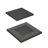
HD6417712BPV Renesas Electronics America, HD6417712BPV Datasheet - Page 364

HD6417712BPV
Manufacturer Part Number
HD6417712BPV
Description
MPU 1.5/3.3V 0K PB-FREE 256-BGA
Manufacturer
Renesas Electronics America
Series
SuperH® SH Ethernetr
Datasheet
1.HD6417712BPV.pdf
(980 pages)
Specifications of HD6417712BPV
Core Processor
SH-3 DSP
Core Size
32-Bit
Speed
200MHz
Connectivity
EBI/EMI, Ethernet, FIFO, SCI, SIO
Peripherals
DMA, POR, WDT
Number Of I /o
24
Program Memory Type
ROMless
Ram Size
16K x 8
Voltage - Supply (vcc/vdd)
1.4 V ~ 1.6 V
Oscillator Type
External
Operating Temperature
-20°C ~ 75°C
Package / Case
256-BGA
Lead Free Status / RoHS Status
Lead free / RoHS Compliant
Eeprom Size
-
Program Memory Size
-
Data Converters
-
Available stocks
Company
Part Number
Manufacturer
Quantity
Price
Company:
Part Number:
HD6417712BPV
Manufacturer:
Renesas Electronics America
Quantity:
10 000
- Current page: 364 of 980
- Download datasheet (6Mb)
Section 11 On-Chip Oscillation Circuits
11.4
The CPG has the following register. For details on register addresses and register access size, refer
to section 23, List of Registers.
• Frequency control register (FRQCR)
11.4.1
The frequency control register (FRQCR) is a 16-bit readable/writable register used to specify
whether a clock is output from the CKIO pin, the frequency multiplication ratio of PLL circuit 1,
and the frequency division ratio of the internal clock and the peripheral clock.
Only word access can be used on the FRQCR register. FRQCR is initialized to H’1003 by a
power-on reset, but retains its value in a manual reset and in standby mode.
The write values to bits 15 to 13, 11 to 10, 7 to 6, and 3 should always be 0.
Rev. 1.00 Dec. 27, 2005 Page 320 of 932
REJ09B0269-0100
Bit
15 to 13
12
11
10
Register Description
Frequency Control Register (FRQCR)
Bit Name
CKOEN
Initial
Value
All 0
1
0
0
R/W
R
R/W
R
R
Description
Reserved
These bits are always read as 0. The write value
should always be 0.
Clock Output Enable
CKOEN specifies whether a clock is output from the
CKIO pin or the CKIO pin is placed in the level-fixed
state in the standby mode, CKIO pin is fixed at low
during STATUS 1 = L, and STATUSO = H, when
CKOEN is set to 0. Therefore, the malfunction of an
external circuit because of an unstable CKIO clock in
releasing the standby mode can be prevented. The
CKIO pin becomes to input pin regardless of the
value of the CKOEN bit in clock operating mode 7.
0: CKIO pin goes to low level state in standby mode.
1: Clock is output from CKIO pin
Reserved
These bits are always read as 0. The write value
should always be 0.
Related parts for HD6417712BPV
Image
Part Number
Description
Manufacturer
Datasheet
Request
R

Part Number:
Description:
KIT STARTER FOR M16C/29
Manufacturer:
Renesas Electronics America
Datasheet:

Part Number:
Description:
KIT STARTER FOR R8C/2D
Manufacturer:
Renesas Electronics America
Datasheet:

Part Number:
Description:
R0K33062P STARTER KIT
Manufacturer:
Renesas Electronics America
Datasheet:

Part Number:
Description:
KIT STARTER FOR R8C/23 E8A
Manufacturer:
Renesas Electronics America
Datasheet:

Part Number:
Description:
KIT STARTER FOR R8C/25
Manufacturer:
Renesas Electronics America
Datasheet:

Part Number:
Description:
KIT STARTER H8S2456 SHARPE DSPLY
Manufacturer:
Renesas Electronics America
Datasheet:

Part Number:
Description:
KIT STARTER FOR R8C38C
Manufacturer:
Renesas Electronics America
Datasheet:

Part Number:
Description:
KIT STARTER FOR R8C35C
Manufacturer:
Renesas Electronics America
Datasheet:

Part Number:
Description:
KIT STARTER FOR R8CL3AC+LCD APPS
Manufacturer:
Renesas Electronics America
Datasheet:

Part Number:
Description:
KIT STARTER FOR RX610
Manufacturer:
Renesas Electronics America
Datasheet:

Part Number:
Description:
KIT STARTER FOR R32C/118
Manufacturer:
Renesas Electronics America
Datasheet:

Part Number:
Description:
KIT DEV RSK-R8C/26-29
Manufacturer:
Renesas Electronics America
Datasheet:

Part Number:
Description:
KIT STARTER FOR SH7124
Manufacturer:
Renesas Electronics America
Datasheet:

Part Number:
Description:
KIT STARTER FOR H8SX/1622
Manufacturer:
Renesas Electronics America
Datasheet:

Part Number:
Description:
KIT DEV FOR SH7203
Manufacturer:
Renesas Electronics America
Datasheet:


