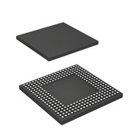
HD6417712BPV Renesas Electronics America, HD6417712BPV Datasheet - Page 481

HD6417712BPV
Manufacturer Part Number
HD6417712BPV
Description
MPU 1.5/3.3V 0K PB-FREE 256-BGA
Manufacturer
Renesas Electronics America
Series
SuperH® SH Ethernetr
Datasheet
1.HD6417712BPV.pdf
(980 pages)
Specifications of HD6417712BPV
Core Processor
SH-3 DSP
Core Size
32-Bit
Speed
200MHz
Connectivity
EBI/EMI, Ethernet, FIFO, SCI, SIO
Peripherals
DMA, POR, WDT
Number Of I /o
24
Program Memory Type
ROMless
Ram Size
16K x 8
Voltage - Supply (vcc/vdd)
1.4 V ~ 1.6 V
Oscillator Type
External
Operating Temperature
-20°C ~ 75°C
Package / Case
256-BGA
Lead Free Status / RoHS Status
Lead free / RoHS Compliant
Eeprom Size
-
Program Memory Size
-
Data Converters
-
Available stocks
Company
Part Number
Manufacturer
Quantity
Price
Company:
Part Number:
HD6417712BPV
Manufacturer:
Renesas Electronics America
Quantity:
10 000
- Current page: 481 of 980
- Download datasheet (6Mb)
Low-Power SDRAM: The low-power SDRAM can be accessed using the same protocol as the
normal SDRAM. The differences between the low-power SDRAM and normal SDRAM are that
partial refresh takes place that puts only a part of the SDRAM in the self-refresh state during the
self-refresh function, and that power consumption is low during refresh under user conditions such
as the operating temperature. The partial refresh is effective in systems in which data in a work
area other than the specific area can be lost without severe repercussions. For details, refer to the
data sheet for the low-power SDRAM to be used.
The low-power SDRAM supports the extension mode register (EMRS) in addition to the mode
registers as the normal SDRAM. This LSI supports issuing of the EMRS command.
The EMRS command is issued according to the conditions specified in table 12.20. For example,
if data H'0YYYYYYY is written to address H’A4FD5XXX in long-word, the commands are
issued to the CS3 space in the following sequence: PALL -> REF x 8 -> MRS -> EMRS. In this
case, the MRS and EMRS issue addresses are H'0000XXX and H'YYYYYYY, respectively. If
data H'1YYYYYYY is written to address H'A4FD5XXX in long-word, the commands are issued
to the CS3 space in the following sequence: PALL -> MRS -> EMRS.
A12/A11*
D31 to D0
A25 to A0
DACKn*
DQMxx
RD/WR
CKIO
RAS
CAS
CSn
BS
1
2
Notes: 1. Address pin to be connected to the A10 pin of SDRAM.
Figure 12.29 Write Timing for SDRAM Mode Register (Based on JEDEC)
2. The waveform for DACKn is when active low is specified.
Tp
PALL
Tpw
REF
Trr
Trc
Trc
REF
Hi-Z
Trr
Rev. 1.00 Dec. 27, 2005 Page 437 of 932
Trc
Section 12 Bus State Controller (BSC)
Trc
MRS
Tmw
REJ09B0269-0100
Tnop
Related parts for HD6417712BPV
Image
Part Number
Description
Manufacturer
Datasheet
Request
R

Part Number:
Description:
KIT STARTER FOR M16C/29
Manufacturer:
Renesas Electronics America
Datasheet:

Part Number:
Description:
KIT STARTER FOR R8C/2D
Manufacturer:
Renesas Electronics America
Datasheet:

Part Number:
Description:
R0K33062P STARTER KIT
Manufacturer:
Renesas Electronics America
Datasheet:

Part Number:
Description:
KIT STARTER FOR R8C/23 E8A
Manufacturer:
Renesas Electronics America
Datasheet:

Part Number:
Description:
KIT STARTER FOR R8C/25
Manufacturer:
Renesas Electronics America
Datasheet:

Part Number:
Description:
KIT STARTER H8S2456 SHARPE DSPLY
Manufacturer:
Renesas Electronics America
Datasheet:

Part Number:
Description:
KIT STARTER FOR R8C38C
Manufacturer:
Renesas Electronics America
Datasheet:

Part Number:
Description:
KIT STARTER FOR R8C35C
Manufacturer:
Renesas Electronics America
Datasheet:

Part Number:
Description:
KIT STARTER FOR R8CL3AC+LCD APPS
Manufacturer:
Renesas Electronics America
Datasheet:

Part Number:
Description:
KIT STARTER FOR RX610
Manufacturer:
Renesas Electronics America
Datasheet:

Part Number:
Description:
KIT STARTER FOR R32C/118
Manufacturer:
Renesas Electronics America
Datasheet:

Part Number:
Description:
KIT DEV RSK-R8C/26-29
Manufacturer:
Renesas Electronics America
Datasheet:

Part Number:
Description:
KIT STARTER FOR SH7124
Manufacturer:
Renesas Electronics America
Datasheet:

Part Number:
Description:
KIT STARTER FOR H8SX/1622
Manufacturer:
Renesas Electronics America
Datasheet:

Part Number:
Description:
KIT DEV FOR SH7203
Manufacturer:
Renesas Electronics America
Datasheet:


