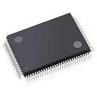
ispPAC-CLK5620AV-01TN100I Lattice, ispPAC-CLK5620AV-01TN100I Datasheet - Page 12

ispPAC-CLK5620AV-01TN100I
Manufacturer Part Number
ispPAC-CLK5620AV-01TN100I
Description
Clock Drivers & Distribution ISP 0 Dlay Clck Gen w/Unv Fan-Out Buf I
Manufacturer
Lattice
Datasheet
1.ISPPAC-CLK5610AV-01TN48I.pdf
(51 pages)
Specifications of ispPAC-CLK5620AV-01TN100I
Minimum Operating Temperature
0 C
Mounting Style
SMD/SMT
Maximum Operating Temperature
70 C
Package / Case
TQFP-100
Lead Free Status / RoHS Status
Lead free / RoHS Compliant
Available stocks
Company
Part Number
Manufacturer
Quantity
Price
Company:
Part Number:
ISPPAC-CLK5620AV-01TN100I
Manufacturer:
LATTICE
Quantity:
210
Company:
Part Number:
ISPPAC-CLK5620AV-01TN100I
Manufacturer:
Lattice Semiconductor Corporation
Quantity:
10 000
Lattice Semiconductor
Performance Characteristics – PLL
f
t
t
t
t
M
N
f
f
V
f
t
t
t
tφ
t
DC
t
PASS
t
t
PSR
1. In PLL Bypass mode (PLL_BYPASS = HIGH), output will support frequencies down to 0Hz (divider chain is a fully static design).
2. Dividers should be set so that they provide the phase detector with signals of 8MHz or greater for loop stability.
3. See Figures 1-3-1-5 for output loads.
4. Input and outputs LVPECL mode
5. Inserted feedback loop delay < 7ns
6. Measured with f
REF,
CLOCKHI,
CLOCKLO
RINP,
FINP
PFD
VCO
OUT
JIT
JIT
JIT(
DELAY
PDBY-
LOCK
RELOCK
Symbol
DIV
DIV
DIV
(cc)
(per)
φ
f
)
FBK
Reference and feedback input
frequency range
Reference and feedback input
clock HIGH and LOW times
Reference and feedback input
rise and fall times
M-divider range
N-Divider range
Phase detector input frequency
range
VCO operating frequency
Output Divider range
Output frequency range
Output adjacent-cycle jitter
(1000 cycle sample)
Output period jitter
(10000 cycle sample)
Reference clock to output jitter
(2000 cycle sample)
Static phase offset
Reference clock to output delay Internal feedback mode
Output duty cycle
Reference clock to output
propagation delay
PLL lock time
PLL relock time
Power supply rejection, period
jitter vs. power supply noise
2
OUT
= 100MHz, f
Parameter
6
5
VCO
1
= 600MHz, input and output interface set to LVPECL.
6
6
M-Divider and N-Divider not
bypassed.
Measured between 20% and 80%
levels
Even integer values only
Fine Skew Mode,
f
Coarse Skew Mode,
f
f
f
f
Output type LVCMOS 3.3V
f
M=1, V=2
From Power-up event
From Reset event
To same reference frequency
To different frequency
f
V
100kHz sinusoidal stimulus
VCO
VCO
PFD
PFD
PFD
OUT
IN
CCA
= f
≥ 100MHz
≥ 100MHz
≥ 100MHz
= 800MHz
>100 MHz
= 800MHz
OUT
= V
CCD
= 100MHz
Conditions
= V
1-12
CCO
All differential
options
All single-ended
options
Input: LVPECL
Output: LVPECL
Input: LVCMOS
Output: LVCMOS
modulated with
4
3
ispClock5600A Family Data Sheet
Min.
1.25
-100
320
2.5
6.2
45
8
1
1
8
2
4
4
6
Typ.
2.25
0.05
150
150
15
15
Max.
8.25
400
400
800
400
266
200
200
8.8
40
40
80
70
12
50
55
5
ps (RMS)
ps (RMS)
ps(RMS)
mV(p-p)
ps (p-p)
Units
MHz
MHz
MHz
MHz
MHz
MHz
ns
ns
ps
ns
ns
ns
µs
µs
µs
µs
%


