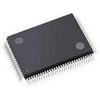
ispPAC-CLK5620AV-01TN100I Lattice, ispPAC-CLK5620AV-01TN100I Datasheet - Page 32

ispPAC-CLK5620AV-01TN100I
Manufacturer Part Number
ispPAC-CLK5620AV-01TN100I
Description
Clock Drivers & Distribution ISP 0 Dlay Clck Gen w/Unv Fan-Out Buf I
Manufacturer
Lattice
Datasheet
1.ISPPAC-CLK5610AV-01TN48I.pdf
(51 pages)
Specifications of ispPAC-CLK5620AV-01TN100I
Minimum Operating Temperature
0 C
Mounting Style
SMD/SMT
Maximum Operating Temperature
70 C
Package / Case
TQFP-100
Lead Free Status / RoHS Status
Lead free / RoHS Compliant
Available stocks
Company
Part Number
Manufacturer
Quantity
Price
Company:
Part Number:
ISPPAC-CLK5620AV-01TN100I
Manufacturer:
LATTICE
Quantity:
210
Company:
Part Number:
ISPPAC-CLK5620AV-01TN100I
Manufacturer:
Lattice Semiconductor Corporation
Quantity:
10 000
Lattice Semiconductor
Internal Feedback Mode
In addition to supporting the use of external feedback to close the phase-locked loop, ispClock5620A also provides
the option of using an internal feedback path for this function. This feature is useful for minimizing external connec-
tions and routing in situations where one can attempt to compensate for external signal path delays using the pro-
grammable skew feature of the internal feedback path.
Profile Select
The ispClock5600A stores all internal configuration data in on-board E
configuration profiles may be stored in each device. The choice of which configuration profile is to be active is spec-
ified thought the profile select inputs PS0 and PS1, as shown in Table 1-5.
Table 1-5. Profile Select Function
Each profile controls the following internal configuration items:
The following settings are independent of the selection of active profile and will apply regardless of which profile is
selected:
If any of the above items are modified, the change will apply across all profiles. In some cases this may cause
unanticipated behavior. If multiple profiles are used in a design, the suitability of the profile independent settings
must be considered with respect to each of the individual profiles.
When a profile is changed by modifying the values of the PS0 and PS1 inputs, it is necessary to assert a RESET
signal to the ispClock5600A to restart the PLL and resynchronize all the internal dividers.
• M-Divider setting
• N-Divider setting
• V-Divider settings
• Output skew settings
• Internal feedback skew settings
• Internal vs. external feedback selection
• Input logic configuration
• Output bank logic configuration
• V-divider to be used as feedback source
• Fine/Coarse skew mode selection
• UES string
– Logic family
– Input impedance
– Logic family
– V-divider signal source
– Enable/SGATE control options
– Output impedance
– Slew rate
– Signal inversion
PS1
0
0
1
1
1-32
PS0
0
1
0
1
Active Profile
Profile 0
Profile 1
Profile 2
Profile 3
ispClock5600A Family Data Sheet
2
CMOS memory. Up to four independent


