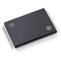
ispPAC-CLK5620AV-01TN100I Lattice, ispPAC-CLK5620AV-01TN100I Datasheet - Page 30

ispPAC-CLK5620AV-01TN100I
Manufacturer Part Number
ispPAC-CLK5620AV-01TN100I
Description
Clock Drivers & Distribution ISP 0 Dlay Clck Gen w/Unv Fan-Out Buf I
Manufacturer
Lattice
Datasheet
1.ISPPAC-CLK5610AV-01TN48I.pdf
(51 pages)
Specifications of ispPAC-CLK5620AV-01TN100I
Minimum Operating Temperature
0 C
Mounting Style
SMD/SMT
Maximum Operating Temperature
70 C
Package / Case
TQFP-100
Lead Free Status / RoHS Status
Lead free / RoHS Compliant
Available stocks
Company
Part Number
Manufacturer
Quantity
Price
Company:
Part Number:
ISPPAC-CLK5620AV-01TN100I
Manufacturer:
LATTICE
Quantity:
210
Company:
Part Number:
ISPPAC-CLK5620AV-01TN100I
Manufacturer:
Lattice Semiconductor Corporation
Quantity:
10 000
Lattice Semiconductor
ispClock5600A Family Data Sheet
coarse mode has a value greater than 40, as the corresponding fine skew mode setting would be greater than 80,
which is not supported.
Output Skew Matching and Accuracy
Understanding the various factors which relate to output skew is essential for realizing optimal skew performance in
the ispClock5600A family of devices.
In the case where two outputs are identically configured, and driving identical loads, the maximum skew is defined
by t
which is specified as a maximum of 50ps. In Figure 1-25 the Bank1A and BANK2A outputs show the
SKEW,
skew error between two matched outputs.
Figure 1-25. Skew Matching Error Sources
2ns +/- (t
) +/- (t
)
SKEW
SKERR
+/- t
SKEW
BANK1A
(skew setting = 0)
BANK2A
(skew setting=0)
BANK3A
(skew setting = 2ns)
One can also program a user-defined skew between two outputs using the skew control units. Because the pro-
grammable skew is derived from the VCO frequency, as described in the previous section, the absolute skew is
very accurate. The typical error for any non-zero skew setting is given by the t
specification. For example, if
SKERR
one is in fine skew mode with a VCO frequency of 500MHz, and selects a skew of 8TU, the realized skew will be
2ns, which will typically be accurate to within +/-30 ps. An example of error vs. skew setting can be found in the
chart ‘Typical Skew Error vs. Setting’ in the typical performance characteristics section. Note that this parameter
adds to output-to-output skew error only if the two outputs have different skew settings. The Bank1A and Bank3A
outputs in Figure 1-25 show how the various sources of skew error stack up in this case. Note that if two or more
outputs are programmed to the same skew setting, then the contribution of the t
skew error term does not
SKERR
apply.
When outputs are configured or loaded differently, this also has an effect on skew matching. If an output is set to sup-
port a different logic type, this can be accounted for by using the t
output adders specified in the Table ‘Switching
IOO
Characteristics’. That table specifies the additional skew added to an output using LVDS as a baseline. For instance, if
one output is specified as LVTTL (t
= 0.395ns), and another output is specified as LVDS (t
= 0ns), then one
IOO
IOO
could expect 0.395ns of additional skew between the two outputs. This timing relationship is shown in Figure 1-26a.
1-30


