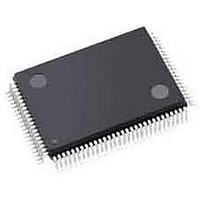
ispPAC-CLK5620AV-01TN100I Lattice, ispPAC-CLK5620AV-01TN100I Datasheet - Page 28

ispPAC-CLK5620AV-01TN100I
Manufacturer Part Number
ispPAC-CLK5620AV-01TN100I
Description
Clock Drivers & Distribution ISP 0 Dlay Clck Gen w/Unv Fan-Out Buf I
Manufacturer
Lattice
Datasheet
1.ISPPAC-CLK5610AV-01TN48I.pdf
(51 pages)
Specifications of ispPAC-CLK5620AV-01TN100I
Minimum Operating Temperature
0 C
Mounting Style
SMD/SMT
Maximum Operating Temperature
70 C
Package / Case
TQFP-100
Lead Free Status / RoHS Status
Lead free / RoHS Compliant
Available stocks
Company
Part Number
Manufacturer
Quantity
Price
Company:
Part Number:
ISPPAC-CLK5620AV-01TN100I
Manufacturer:
LATTICE
Quantity:
210
Company:
Part Number:
ISPPAC-CLK5620AV-01TN100I
Manufacturer:
Lattice Semiconductor Corporation
Quantity:
10 000
Lattice Semiconductor
When GOE is HIGH, all output drivers are forced into a high-Z state, regardless of any internal configuration. When
GOE is LOW, the output drivers may also be enabled or disabled on an individual basis, and optionally controlled
by the OEX and OEY pins. Internal E
enabled (when GOE pin is LOW), never enabled (permanently off), or selectively enabled by the state of either
OEX or OEY.
Synchronous output gating is provided by ispClock5600A devices through the use of the SGATE pin. The SGATE
pin does not disable the output driver, but merely forces the output to either a high or low state, depending on the
output driver’s polarity setting. If the output driver polarity is true, the output will be forced LOW when SGATE is
brought LOW, while if it is inverted, the output will be forced HIGH. A primary feature of the SGATE function is that
the clock output is enabled and disabled synchronous to the selected internal clock source. This prevents the gen-
eration of partial, ‘runt’, output clock pulses, which would otherwise occur with simple combinatorial gating
schemes. The SGATE is available to all clock outputs and is selectable on a bank-by-bank basis.
Table 1-3 shows the behavior of the outputs for various combinations of the output enables, SGATE input, and
E
Table 1-3. Clock Output Enable Functions
Table 1-4. SGATE Function
Skew Control Units
Each of the ispClock5600A’s clock outputs is supported by a skew control unit which allows the user to insert an
individually programmable delay into each output signal. This feature is useful when it is necessary to de-skew
clock signals to compensate for physical length variations among different PCB clock paths.
Unlike the skew adjustment features provided in many competing products, the ispClock5600A’s skew adjustment
feature provides exact and repeatable delays which exhibit extremely low channel-to-channel and device-to-device
variation. This is achieved by deriving all skew timing from the VCO, which results in the skew increment being a lin-
ear function of the VCO period. For this reason, skews are defined in terms of ‘unit delays’, which may be pro-
grammed by the user over a range of 0 to 15. The ispClock5600A family also supports both ‘fine’ and ‘coarse’ skew
modes. In fine skew mode, the unit skew ranges from 156ps to 390 ps, while in the coarse skew mode unit skew
varies from 312ps to 780ps. The exact unit skew (TU) may be calculated from the VCO frequency (f
the following expressions:
2
CMOS configuration.
SGATE Bank Controlled by SGATE?
X
X
0
0
1
1
GOE
X
0
0
0
0
0
1
OEX
X
X
X
X
X
0
1
2
CMOS configuration is used to establish whether the output driver is always
YES
YES
YES
YES
NO
NO
OEY
X
X
X
X
X
0
1
E
Enable on OEX
Enable on OEX
Enable on OEY
Enable on OEY
2
Always OFF
Configuration
Always ON
1-28
n/a
Output Polarity
Inverted
Inverted
Inverted
True
True
True
ispClock5600A Family Data Sheet
Clock Out
Clock Out
Clock Out
Output
High-Z
High-Z
High-Z
High-Z
Inverted Clock
Inverted Clock
Output
Clock
HIGH
Clock
LOW
vco
) by using


