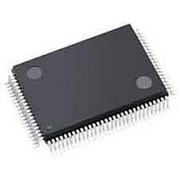
ispPAC-CLK5620AV-01TN100I Lattice, ispPAC-CLK5620AV-01TN100I Datasheet - Page 21

ispPAC-CLK5620AV-01TN100I
Manufacturer Part Number
ispPAC-CLK5620AV-01TN100I
Description
Clock Drivers & Distribution ISP 0 Dlay Clck Gen w/Unv Fan-Out Buf I
Manufacturer
Lattice
Datasheet
1.ISPPAC-CLK5610AV-01TN48I.pdf
(51 pages)
Specifications of ispPAC-CLK5620AV-01TN100I
Minimum Operating Temperature
0 C
Mounting Style
SMD/SMT
Maximum Operating Temperature
70 C
Package / Case
TQFP-100
Lead Free Status / RoHS Status
Lead free / RoHS Compliant
Available stocks
Company
Part Number
Manufacturer
Quantity
Price
Company:
Part Number:
ISPPAC-CLK5620AV-01TN100I
Manufacturer:
LATTICE
Quantity:
210
Company:
Part Number:
ISPPAC-CLK5620AV-01TN100I
Manufacturer:
Lattice Semiconductor Corporation
Quantity:
10 000
Lattice Semiconductor
Figure 1-14. ispClock5600A Clock Reference and Feedback Input Structure (REFA+/- Pair Shown)
The following usage guidelines are suggested for interfacing to supported logic families.
LVTTL (3.3V), LVCMOS (1.8V, 2.5V, 3.3V)
The receiver should be set to LVCMOS or LVTTL mode, and the input signal should be connected to the ‘+’ termi-
nal of the input pair (e.g. REFA+). The ‘-’ input terminal should be connected to GND. In addition, REFVTT should
also be tied to GND. CMOS transmission lines are generally source terminated, so all termination resistors should
be set to the OPEN state. Figure 1-15 shows the proper configuration. Please note that because switching thresh-
olds are different for LVCMOS running at 1.8V, there is a separate configuration setting for this particular standard.
Figure 1-15. LVCMOS/LVTTL Input Receiver Configuration
HSTL, eHSTL, SSTL2, SSTL3
The receiver should be set to HSTL/SSTL mode, and the input signal should be fed into the ‘+’ terminal of the input
pair. The ‘-’ input terminal should be tied to the appropriate V
terminal should be tied to a V
set to 50Ω. Figure 1-16 shows an appropriate configuration. Refer to the “Recommended Operating Conditions -
Supported Logic Standards” table in this data sheet for suitable values of V
REFVTT
REFA+
REFA-
TT
ispClock5600A
termination supply. The positive input’s terminating resistor should be engaged and
R
T
Signal In
GND
GND
REFVTT
REFA+
REFA-
R
T
ispClock5600A
R
T
OPEN
1-21
Single-ended
Differential
Receiver
Receiver
REF
value, and the associated REFVTT or FBKVTT
ispClock5600A Family Data Sheet
Single-ended
Receiver
REF
To Internal
and V
Logic
TT.
If one of the REF or FBK


