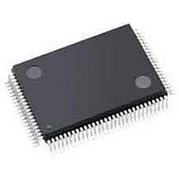
ispPAC-CLK5620AV-01TN100I Lattice, ispPAC-CLK5620AV-01TN100I Datasheet - Page 24

ispPAC-CLK5620AV-01TN100I
Manufacturer Part Number
ispPAC-CLK5620AV-01TN100I
Description
Clock Drivers & Distribution ISP 0 Dlay Clck Gen w/Unv Fan-Out Buf I
Manufacturer
Lattice
Datasheet
1.ISPPAC-CLK5610AV-01TN48I.pdf
(51 pages)
Specifications of ispPAC-CLK5620AV-01TN100I
Minimum Operating Temperature
0 C
Mounting Style
SMD/SMT
Maximum Operating Temperature
70 C
Package / Case
TQFP-100
Lead Free Status / RoHS Status
Lead free / RoHS Compliant
Available stocks
Company
Part Number
Manufacturer
Quantity
Price
Company:
Part Number:
ISPPAC-CLK5620AV-01TN100I
Manufacturer:
LATTICE
Quantity:
210
Company:
Part Number:
ISPPAC-CLK5620AV-01TN100I
Manufacturer:
Lattice Semiconductor Corporation
Quantity:
10 000
Lattice Semiconductor
ispClock5600A Family Data Sheet
actual impedance required will be a function of the driver used to generate the signal and the transmission medium
used (PCB traces, connectors and cabling). The ispClock5600A’s ability to adjust input impedance over a range of
40Ω to 70Ω allows the user to adapt his circuit to non-ideal behaviors from the rest of the system without having to
swap out components.
Output Drivers
The ispClock5600A provide banks of configurable, internally-terminated high-speed dual-output line drivers. The
ispClock5610A provides five driver banks, while the ispClock5620A provides ten. Each of these driver banks may
be configured to provide either a single differential output signal, or a pair of single-ended output signals. Program-
mable internal source-series termination allows the ispClock5600A to be matched to transmission lines with imped-
2
ances ranging from 40 to 70 Ohms. The outputs may be independently enabled or disabled, either from E
CMOS
configuration or by external control lines. Additionally, each can be independently programmed to provide a fixed
amount of signal delay or skew, allowing the user to compensate for the effects of unequal PCB trace lengths or
loading effects. Figure 1-20 shows a block diagram of a typical ispClock5600A output driver bank and associated
skew control.
Because of the high edge rates which can be generated by the ispClock5600A’s clock output drivers, the VCCO
power supply pin for each output bank should be individually bypassed. Low ESR capacitors with values ranging
from 0.01 to 0.1 µF may be used for this purpose. Each bypass capacitor should be placed as close to its respec-
tive output bank power pins (VCCO and GNDO) pins as is possible to minimize interconnect length and associated
parasitic inductances.
In the case where an output bank is unused, the associated VCCO pin may be either left floating or tied to ground
to reduce quiescent power consumption. We recommend, however, that all unused VCCO pins be tied to ground
where possible. All GND0 pins must be tied to ground, regardless of whether or not the associated bank is used.
1-24


