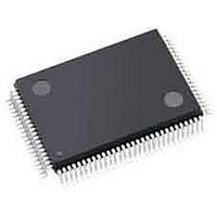
ispPAC-CLK5620AV-01TN100I Lattice, ispPAC-CLK5620AV-01TN100I Datasheet - Page 26

ispPAC-CLK5620AV-01TN100I
Manufacturer Part Number
ispPAC-CLK5620AV-01TN100I
Description
Clock Drivers & Distribution ISP 0 Dlay Clck Gen w/Unv Fan-Out Buf I
Manufacturer
Lattice
Datasheet
1.ISPPAC-CLK5610AV-01TN48I.pdf
(51 pages)
Specifications of ispPAC-CLK5620AV-01TN100I
Minimum Operating Temperature
0 C
Mounting Style
SMD/SMT
Maximum Operating Temperature
70 C
Package / Case
TQFP-100
Lead Free Status / RoHS Status
Lead free / RoHS Compliant
Available stocks
Company
Part Number
Manufacturer
Quantity
Price
Company:
Part Number:
ISPPAC-CLK5620AV-01TN100I
Manufacturer:
LATTICE
Quantity:
210
Company:
Part Number:
ISPPAC-CLK5620AV-01TN100I
Manufacturer:
Lattice Semiconductor Corporation
Quantity:
10 000
Lattice Semiconductor
Each of the ispClock5600A’s output driver banks can be configured to support the following logic outputs:
To provide LVTTL, LVCMOS, SSTL2, SSTL3, HSTL and eHSTL outputs, the CMOS output drivers in each bank are
enabled. These circuits provide logic outputs which swing from ground to the VCCO supply rail. The choice of
VCCO to be supplied to a given bank is determined by the logic standard to which that bank is configured. Because
each pair of outputs has its own VCCO supply pin, each bank can be independently configured to support a differ-
ent logic standard. Note that the two outputs associated with a bank must necessarily be configured to the same
logic standard. The source impedance of each of the two outputs in each bank may be independently set over a
range of 40Ω to 70Ω in 5Ω steps. A low impedance option (≈20Ω) is also provided for cases where low source ter-
mination is desired on a given output.
Control of output slew rate is also provided in LVTTL, LVCMOS, SSTL2, SSTL3, HSTL and eHSTL output modes.
Four output slew-rate settings are provided, as specified in the “Output Rise Times” and “Output Fall Times” tables
in this data sheet.
To provide LVDS and differential LVPECL outputs, a separate internal driver is used which provides the correct
LVDS or LVPECL logic levels when operating from a 3.3V VCCO. Because both LVDS and differential LVPECL
transmission lines are normally terminated with a single 100Ω resistor between the ‘+’ and ‘-’ signal lines at the far
end, the ispClock5600A’s internal termination resistors are not available in these modes. Also note that output
slew-rate control is not available in LVDS or LVPECL mode, and that these drivers always operate at a fixed slew-
rate.
Polarity control (true/inverted) is available for all output drivers. In the case of single-ended output standards, the
polarity of each of the two output signals from each bank may be controlled independently. In the case of differen-
tial output standards, the polarity of the differential pair may be selected.
Suggested Usage
Figure 1-21 shows a typical configuration for the ispClock5600A’s output driver when configured to drive an LVTTL
or LVCMOS load. The ispClock5600A’s output impedance should be set to match the characteristic impedance of
the transmission line being driven. The far end of the transmission line should be left open, with no termination
resistors.
Figure 1-21. Configuration for LVTTL/LVCMOS Output Modes
• LVTTL
• LVCMOS (1.8V, 2.5V, 3.3V)
• SSTL2
• SSTL3
• HSTL
• eHSTL
• LVDS
• Differential LVPECL (3.3V)
• Differential SSTL18, SSTL2, SSTL3, HSTL, eHSTL
LVCMOS/LVTTL
Mode
ispClock5600A
Ro = Zo
1-26
Zo
ispClock5600A Family Data Sheet
LVCMOS/LVTTL
Receiver


