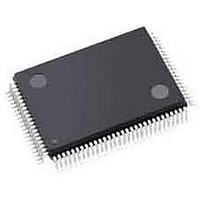
ispPAC-CLK5620AV-01TN100I Lattice, ispPAC-CLK5620AV-01TN100I Datasheet - Page 33

ispPAC-CLK5620AV-01TN100I
Manufacturer Part Number
ispPAC-CLK5620AV-01TN100I
Description
Clock Drivers & Distribution ISP 0 Dlay Clck Gen w/Unv Fan-Out Buf I
Manufacturer
Lattice
Datasheet
1.ISPPAC-CLK5610AV-01TN48I.pdf
(51 pages)
Specifications of ispPAC-CLK5620AV-01TN100I
Minimum Operating Temperature
0 C
Mounting Style
SMD/SMT
Maximum Operating Temperature
70 C
Package / Case
TQFP-100
Lead Free Status / RoHS Status
Lead free / RoHS Compliant
Available stocks
Company
Part Number
Manufacturer
Quantity
Price
Company:
Part Number:
ISPPAC-CLK5620AV-01TN100I
Manufacturer:
LATTICE
Quantity:
210
Company:
Part Number:
ISPPAC-CLK5620AV-01TN100I
Manufacturer:
Lattice Semiconductor Corporation
Quantity:
10 000
Lattice Semiconductor
RESET and Power-up Functions
To ensure proper PLL startup and synchronization of outputs, the ispClock5600A provides both internally gener-
ated and user-controllable external reset signals. An internal reset is generated whenever the device is powered
up. An external reset may be applied by asserting a logic HIGH at the RESET pin. Asserting RESET resets all
internal dividers, and will cause the PLL to lose lock. On losing lock, the VCO frequency will begin dropping. The
length of time required to regain lock is related to the length of time for which RESET was asserted.
When the ispClock5600A begins operating from initial power-on, the VCO starts running at a very low frequency
(<100 MHz) which gradually increases as it approaches a locked condition. To prevent invalid outputs from being
applied to the rest of the system, it is recommended that either the SGATE, OEX, or OEY pins be used to control
the outputs based on the status of the LOCK pin. Holding the SGATE pin LOW during power-up will result in the
BANK outputs being asserted HIGH or LOW (depending on inversion status) until SGATE is brought HIGH. Assert-
ing OEX or OEY high will result in the BANK outputs being held in a high-impedance state until the OEX or OEY
pin is pulled LOW.
When either of the minimum t
insure proper behavior of the PLL and outputs.
Thermal Management
In applications where a majority of the ispClock5610A or ispClock5620A’s outputs are active and operating at or
near maximum output frequency (266MHz for single ended and 400MHz for differential outputs), package thermal
limitations may need to be considered to ensure a successful design. Thermal characteristics of the packages
employed by Lattice Semiconductor may be found in the document Thermal Management which may be obtained
at www.latticesemi.com.
The maximum current consumption of the digital and analog core circuitry for ispClock5620A is 150mA worst case
(I
MHz, both outputs in each bank enabled). This results in a total device dissipation:
With a maximum recommended operating junction temperature (T
maximum allowable ambient temperature (T
where Θ
The above analysis represents the worst-case scenario. Significant improvement in maximum ambient operating
temperature can be realized with additional cooling. Providing a 200 LFM (Linear Feet per Minute) airflow reduces
Θ
In practice, however, the absolute worst-case situation will be relatively rare, as not all outputs may be running at
maximum output frequency in a given application. Additionally, if the internal VCO is operating at less than its max-
imum frequency (800MHz), it requires less current on the VCCD pin. In these situations, one can estimate the
effective I
VCO frequency. Normalized curves relating current to operating frequency for these parameters may be found in
the Typical Performance Characteristics section.
While it is possible to perform detailed calculations to estimate the maximum ambient operating temperature from
operating conditions, some simpler rule-of-thumb guidance can also be obtained through the derating curves
shown in Figure 1-28. The curves in Figure 1-28a show the maximum ambient operating temperature permitted
when operating a given number of output banks at the maximum output frequency (266MHz for single ended and
400MHz for differential outputs). Note that it is assumed that both outputs in each bank are active.
CCD
JA
to 33°C/W for the 100 TQFP package, which results in a maximum ambient operating temperature of 71°C.
+ I
JA
CCA
CCO
= 36.9°C/W for the 100 TQFP package. Θ
), and each of the output banks may draw up to 38mA worst case (LVCMOS 3.3V, CL=5pF, f
for each bank and the effective I
T
AMAX
CLOCKHI
= T
P
JOP
DMAX
- PD
or t
= 3.3V x (10 x 38mA + 150mA) = 1.75W
CLOCKLO
MAX
AMAX
x Θ
CCD
) can be estimated as
JA
specifications is violated, the RESET pin should be activated to
= 130°C - 1.75W x 36.9°C/W = 65.4°C
JA
for the digital core functions based on output frequency and
1-33
= 68°C/W for the 48 TQFP package in still air.
JOP
) of 130°C for an industrial grade device, the
ispClock5600A Family Data Sheet
OUT
=266
(3)
(4)


