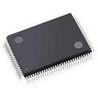
ispPAC-CLK5620AV-01TN100I Lattice, ispPAC-CLK5620AV-01TN100I Datasheet - Page 40

ispPAC-CLK5620AV-01TN100I
Manufacturer Part Number
ispPAC-CLK5620AV-01TN100I
Description
Clock Drivers & Distribution ISP 0 Dlay Clck Gen w/Unv Fan-Out Buf I
Manufacturer
Lattice
Datasheet
1.ISPPAC-CLK5610AV-01TN48I.pdf
(51 pages)
Specifications of ispPAC-CLK5620AV-01TN100I
Minimum Operating Temperature
0 C
Mounting Style
SMD/SMT
Maximum Operating Temperature
70 C
Package / Case
TQFP-100
Lead Free Status / RoHS Status
Lead free / RoHS Compliant
Available stocks
Company
Part Number
Manufacturer
Quantity
Price
Company:
Part Number:
ISPPAC-CLK5620AV-01TN100I
Manufacturer:
LATTICE
Quantity:
210
Company:
Part Number:
ISPPAC-CLK5620AV-01TN100I
Manufacturer:
Lattice Semiconductor Corporation
Quantity:
10 000
Lattice Semiconductor
Figure 1-33. ispClock5600A Family ID Codes
In addition to the four instructions described above, there are 20 unique instructions specified by Lattice for the
ispClock5600A. These instructions are primarily used to interface to the various user registers and the E
non-volatile memory. Additional instructions are used to control or monitor other features of the device, including
boundary scan operations. A brief description of each unique instruction is provided in detail below, and the bit
codes are found in Table 1-6.
PROGRAM_ENABLE – This instruction enables the ispClock5600A’s programming mode.
PROGRAM_DISABLE – This instruction disables the ispClock5600A’s programming mode.
BULK_ERASE – This instruction will erase all E
security fuse (ESF). A bulk erase instruction must be issued before reprogramming a device. The device must
already be in programming mode for this instruction to execute.
ADDRESS_SHIFT – This instruction shifts address data into the address register (10 bits) in preparation for either
a PROGRAM or VERIFY instruction.
DATA_SHIFT – This instruction shifts data into or out of the data register (90 bits), and is used with both the PRO-
GRAM and VERIFY instructions.
PROGRAM – This instruction programs the contents of the data register to the E
to by the address register. The device must already be in programming mode for this instruction to execute.
PROG_INCR – This instruction first programs the contents of the data register into E
pointed to by the address register and then auto-increments the value of the address register. The device must
already be in programming mode for this instruction to execute.
PROGRAM_SECURITY – This instruction programs the electronic security fuse (ESF). This prevents data other
than the ID code and UES strings from being read from the device. The electronic security fuse may only be reset
by issuing a BULK_ERASE command. The device must already be in programming mode for this instruction to exe-
cute.
VERIFY – This instruction loads data from the E
shifted out. The device must already be in programming mode for this instruction to execute.
E
E
2
2
Configured
Configured
Version
Version
(4 bits)
(4 bits)
0166h = ispClock5610A
0167h = ispClock5620A
MSB
MSB
(3.3V version)
(3.3V version)
Part Number
Part Number
XXXX / 0000 0001 0110 0110 / 0000 0100 001 / 1
XXXX / 0000 0001 0110 0111 / 0000 0100 001 / 1
(16 bits)
(16 bits)
2
CMOS bits in the device, including the UES data and electronic
2
CMOS array into the column register. The data may then be
1-40
Lattice Semiconductor
Lattice Semiconductor
JEDEC Manufacturer
JEDEC Manufacturer
Identity Code for
Identity Code for
(11 bits)
(11 bits)
ispClock5600A Family Data Sheet
LSB
LSB
per 1149.1-1990
per 1149.1-1990
Constant ‘1’
Constant ‘1’
2
CMOS memory column pointed
(1 bit)
(1 bit)
2
CMOS memory column
2
CMOS


