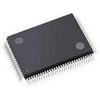
ispPAC-CLK5620AV-01TN100I Lattice, ispPAC-CLK5620AV-01TN100I Datasheet - Page 34

ispPAC-CLK5620AV-01TN100I
Manufacturer Part Number
ispPAC-CLK5620AV-01TN100I
Description
Clock Drivers & Distribution ISP 0 Dlay Clck Gen w/Unv Fan-Out Buf I
Manufacturer
Lattice
Datasheet
1.ISPPAC-CLK5610AV-01TN48I.pdf
(51 pages)
Specifications of ispPAC-CLK5620AV-01TN100I
Minimum Operating Temperature
0 C
Mounting Style
SMD/SMT
Maximum Operating Temperature
70 C
Package / Case
TQFP-100
Lead Free Status / RoHS Status
Lead free / RoHS Compliant
Available stocks
Company
Part Number
Manufacturer
Quantity
Price
Company:
Part Number:
ISPPAC-CLK5620AV-01TN100I
Manufacturer:
LATTICE
Quantity:
210
Company:
Part Number:
ISPPAC-CLK5620AV-01TN100I
Manufacturer:
Lattice Semiconductor Corporation
Quantity:
10 000
Lattice Semiconductor
Figure 1-28. Maximum Ambient Temperature vs. Number of Active Output Banks
Figure 1-28b shows another derating curve, derived under the assumption that the output frequency is 100MHz.
For many applications, 100MHz outputs will be a more realistic scenario. Comparing the maximum temperature
limits of Figure 1-28b with Figure 1-28a, one can see that significantly higher operating temperatures are possible
in LVCMOS 3.3V output mode with more outputs at 100MHz than at 400MHz.
The examples above used LVCMOS 3.3V logic, which represents the maximum power dissipation case at higher
frequencies. For optimal operation at very high frequencies (> 150 MHz) LVDS/LVPECL will often be the best
choice from a signal integrity standpoint. For LVDS-configured outputs, the maximum ICCO current consumption
per bank is low enough that both the ispClock5610A and ispClock5620A can operate all outputs at maximum fre-
quency over their complete rated temperature range, as shown in Figure 1-28c.
Note that because of variations in circuit board mounting, construction, and layout, as well as convective and forced
airflow present in a given design, actual die operating temperature is subject to considerable variation from that
which may be theoretically predicted from package characteristics and device power dissipation.
Software-Based Design Environment
Designers can configure the ispClock5600A using Lattice’s PAC-Designer software, an easy to use, Microsoft Win-
dows compatible program. Circuit designs are entered graphically and then verified, all within the PAC-Designer envi-
ronment. Full device programming is supported using PC parallel port I/O operations and a download cable
connected to the serial programming interface pins of the ispClock5600A. A library of configurations is included with
basic solutions and examples of advanced circuit techniques are available. In addition, comprehensive on-line and
printed documentation is provided that covers all aspects of PAC-Designer operation. PAC-Designer is available for
download from the Lattice website at www.latticesemi.com. The PAC-Designer schematic window, shown in Figure 1-
29 provides access to all configurable ispClock5600A elements via its graphical user interface. All analog input and
output pins are represented. Static or non-configurable pins such as power, ground and the serial digital interface are
omitted for clarity. Any element in the schematic window can be accessed via mouse operations as well as menu
commands. When completed, configurations can be saved and downloaded to devices.
90
80
70
60
50
40
30
0
(Outputs LVCMOS33 3.3V, f
5620A Industrial
5620A Commercial
5610A Industrial
5610A Commercial
2
Temperature Derating Curves
# Active Output Banks
4
6
OUT
8
= 100 MHz)
10
12
1-34
90
85
80
75
70
65
60
0
ispClock5600A Family Data Sheet
(Outputs LVDS, f
Temperature Derating Curves
2
# Active Output Banks
4
OUT
6
= 400 MHz)
8
10


