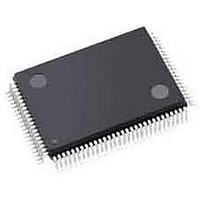
ispPAC-CLK5620AV-01TN100I Lattice, ispPAC-CLK5620AV-01TN100I Datasheet - Page 19

ispPAC-CLK5620AV-01TN100I
Manufacturer Part Number
ispPAC-CLK5620AV-01TN100I
Description
Clock Drivers & Distribution ISP 0 Dlay Clck Gen w/Unv Fan-Out Buf I
Manufacturer
Lattice
Datasheet
1.ISPPAC-CLK5610AV-01TN48I.pdf
(51 pages)
Specifications of ispPAC-CLK5620AV-01TN100I
Minimum Operating Temperature
0 C
Mounting Style
SMD/SMT
Maximum Operating Temperature
70 C
Package / Case
TQFP-100
Lead Free Status / RoHS Status
Lead free / RoHS Compliant
Available stocks
Company
Part Number
Manufacturer
Quantity
Price
Company:
Part Number:
ISPPAC-CLK5620AV-01TN100I
Manufacturer:
LATTICE
Quantity:
210
Company:
Part Number:
ISPPAC-CLK5620AV-01TN100I
Manufacturer:
Lattice Semiconductor Corporation
Quantity:
10 000
Lattice Semiconductor
The input, or M-Divider prescales the input reference frequency, and can be programmed with integer values over
the range of 1 to 40. To achieve low levels of output jitter, it is best to use the smallest M-Divider value possible.
The feedback, or N-Divider prescales the feedback frequency and like the M-Divider, can also be programmed with
integer values ranging from 1 to 40.
Each one of the five output, or V-Dividers can be independently programmed to provide even division ratios ranging
from 2 to 80.
When the PLL is selected (PLL_BYPASS=LOW) and locked, the output frequency of each V-Divider (f
calculated as:
where
Note that because the feedback may be taken from any V-Divider, V
Because the VCO has an operating frequency range spanning 320 MHz to 800 MHz, and the V-Dividers provide
division ratios from 2 to 80, the ispClock5600A can generate output signals ranging from 5 MHz to 400 MHz. For
performance and stability reasons, however, there are several constraints which should be followed when selecting
divider values:
M-Divider and N-Divider Bypass Mode
The M-Divider and the N-Divider in the ispClock5600A device can be bypassed using PAC-Designer software. M
and N-Dividers should be bypassed in applications that require glitchless switching between reference and feed-
back clocks. However, the frequencies of these clocks should be close. If M and N-Dividers are not bypassed, one
should ensure that t
is necessary to ensure reliable switchover.
Figure 1-13. M-Divider and N-Divider Bypass Mode
f
f
M and N are the input and feedback divider settings
V
V
• Use the smallest feasible value for the M-Divider
• The product of the N-Divider and the V-Divider used to close the PLL’s feedback loop should be less than or
k
ref
fbk
k
• The output frequency from the M (and N) divider should be greater or equal to 8 MHz.
equal to 80 (N x V
is the frequency of V-Divider k
is the setting of the V-Divider used to provide output k
is the input reference frequency
is the setting of the V-Divider used to close the PLL feedback path
CLOCKHI
REFSEL
FBKSEL
REFB
REFA
FBKA
FBKB
fbk
≤ 80)
and t
CLOCKLO
specifications are not violated. Otherwise, activation of the reset signal
f
k
=
M-Divider Bypass
N-Divider Bypass
f
M-Divider
N-Divider
ref
1-19
N x V
M x V
fbk
k
k
and V
ispClock5600A Family Data Sheet
fbk
may refer to the same divider.
PFD
k
) may be
(1)


