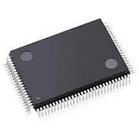
ispPAC-CLK5620AV-01TN100I Lattice, ispPAC-CLK5620AV-01TN100I Datasheet - Page 20

ispPAC-CLK5620AV-01TN100I
Manufacturer Part Number
ispPAC-CLK5620AV-01TN100I
Description
Clock Drivers & Distribution ISP 0 Dlay Clck Gen w/Unv Fan-Out Buf I
Manufacturer
Lattice
Datasheet
1.ISPPAC-CLK5610AV-01TN48I.pdf
(51 pages)
Specifications of ispPAC-CLK5620AV-01TN100I
Minimum Operating Temperature
0 C
Mounting Style
SMD/SMT
Maximum Operating Temperature
70 C
Package / Case
TQFP-100
Lead Free Status / RoHS Status
Lead free / RoHS Compliant
Available stocks
Company
Part Number
Manufacturer
Quantity
Price
Company:
Part Number:
ISPPAC-CLK5620AV-01TN100I
Manufacturer:
LATTICE
Quantity:
210
Company:
Part Number:
ISPPAC-CLK5620AV-01TN100I
Manufacturer:
Lattice Semiconductor Corporation
Quantity:
10 000
Lattice Semiconductor
Note: Bypassing M- and N-Dividers also results in reducing the number of output frequency combinations gener-
ated from a single reference clock input.
PLL_BYPASS Mode
The PLL_BYPASS mode is provided so that input reference signals can be coupled through to the outputs without
using the PLL functions. When PLL_BYPASS mode is enabled (PLL_BYPASS=HIGH), the output of the M-Divider
is routed directly to the inputs of the V-Dividers. In PLL_BYPASS mode, the nominal values of the V-Dividers are
halved, so that they provide division ratios ranging from 1 to 40. The output frequency for a given V-Divider (f
be determined by
Please note that PLL_BYPASS mode is provided primarily for testing purposes. When PLL_BYPASS mode is
enabled, features such as lock detect and skew generation are unavailable.
Reference and External Feedback Inputs
The ispClock5600A provides sets of configurable, internally-terminated inputs for both clock reference and feed-
back signals. In normal operation, one of the clock reference input pairs (REFA+/- or REFB+/-) is used as a clock
input.
The external feedback inputs make it possible to compensate for input to output delay through external means. This
makes it possible to provide output clocks which have very low skews in relation to the reference clock regardless
of loading effects.
The ispClock5610A provides one input signal pair for reference input and one input pair for external feedback,
while the ispClock5620A provides two pairs for reference signals and two pairs for feedback. To select between ref-
erence and feedback inputs, the ispClock5620A provides two CMOS-compatible digital inputs called REFSEL and
FBKSEL. Table 1-2 shows the behavior of these two control inputs.
Table 1-2. REFSEL and FBKSEL Operation for ispClock5620A
Each input also features internal programmable termination resistors, as shown in Figure 1-14. Note that all refer-
ence inputs (REFA+, REFA-, REFB+, REFB-) terminate to the REFVTT pin, while all feedback inputs (FBKA+,
FBKA-, FBKB+, FBKB-) terminate to the FBKVTT pin.
• LVTTL (3.3V)
• LVCMOS (1.8V, 2.5V, 3.3V)
• SSTL2
• SSTL3
• HSTL
• eHSTL
• Differential SSTL1.8
• Differential SSTL2
• Differential SSTL3
• Differential HSTL
• LVDS
• LVPECL (differential, 3.3V)
REFSEL
0
1
Input Pair
Selected
REFB+/-
REFA+/-
f
k
=
1-20
f
M x V
ref
x 2
FBKSEL
k
0
1
ispClock5600A Family Data Sheet
Input Pair
Selected
FBKA+/-
FBKB+/-
k
) will
(2)


