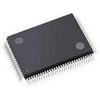
ispPAC-CLK5620AV-01TN100I Lattice, ispPAC-CLK5620AV-01TN100I Datasheet - Page 18

ispPAC-CLK5620AV-01TN100I
Manufacturer Part Number
ispPAC-CLK5620AV-01TN100I
Description
Clock Drivers & Distribution ISP 0 Dlay Clck Gen w/Unv Fan-Out Buf I
Manufacturer
Lattice
Datasheet
1.ISPPAC-CLK5610AV-01TN48I.pdf
(51 pages)
Specifications of ispPAC-CLK5620AV-01TN100I
Minimum Operating Temperature
0 C
Mounting Style
SMD/SMT
Maximum Operating Temperature
70 C
Package / Case
TQFP-100
Lead Free Status / RoHS Status
Lead free / RoHS Compliant
Available stocks
Company
Part Number
Manufacturer
Quantity
Price
Company:
Part Number:
ISPPAC-CLK5620AV-01TN100I
Manufacturer:
LATTICE
Quantity:
210
Company:
Part Number:
ISPPAC-CLK5620AV-01TN100I
Manufacturer:
Lattice Semiconductor Corporation
Quantity:
10 000
Lattice Semiconductor
Lock Detect mode. In Phase Lock Detect mode, the LOCK signal is asserted if the phases of the reference and
feedback signals match, whereas in Frequency Lock Detect mode the LOCK signal is asserted when the frequen-
cies of the feedback and reference signals match. The option for which mode to use is programmable and may be
set using PAC-Designer software (available from the Lattice website at www.latticesemi.com).
In Phase Lock Detect mode the lock detector asserts the LOCK signal as soon as a lock condition is determined.
In Frequency Lock Detect mode, however, the PLL must be in a locked condition for a set number of phase detector
cycles before the LOCK signal will be asserted. The number of cycles required before asserting the LOCK signal in
frequency-lock mode can be set from 16 to 256.
When the lock condition is lost the LOCK signal will be de-asserted immediately in both Phase Lock Detect and
Frequency Lock Detect modes.
Loop Filter: The loop filter parameters for each profile are automatically selected by the PAC-Designer software
depending on the following:
Spread Spectrum Support: The reference clock inputs of the ispClock5600A device are spread spectrum clock
tolerant. The tolerance limits are:
Figure 1-12. PLL Loop Bandwidth vs. Feedback Divider Setting (Nominal)
VCO
The ispClock5600A provides an internal VCO which provides an output frequency ranging from 320MHz to
800MHz. The VCO is implemented using differential circuit design techniques which minimize the influence of
power supply noise on measured output jitter. The VCO is also used to generate output clock skew as a function of
the total VCO period. Using the VCO as the basis for controlling output skew allows for highly precise and consis-
tent skew generation, both from device-to-device, as well as channel-to-channel within the same device.
M-, N-, and V-Dividers
The ispClock5600A incorporates a set of programmable dividers which provide the ability to synthesize output fre-
quencies differing from that of the reference clock input.
• Individual profile VCO operating frequency
• Individual profile NxV product
• Maximum VCO operating frequency across all used profiles
• Center spread ±0.125% to ±2%
• Down spread -0.25% to -4%
• 30-33kHz modulation frequency
7
6
5
4
3
2
1
0
0
PLL Loop Bandwidth vs. Feedback
Divider Setting in Standard Mode
N x V Feedback Division Product
20
40
60
80
1-18
Setting in Spread-Spectrum Compliant Mode
7
6
5
4
3
2
1
0
PLL Loop Bandwidth vs. Feedback Divider
0
N x V Feedback Division Product
ispClock5600A Family Data Sheet
20
40
60
80


