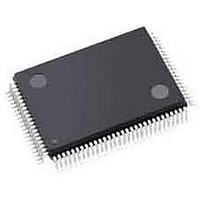
ispPAC-CLK5620AV-01TN100I Lattice, ispPAC-CLK5620AV-01TN100I Datasheet - Page 39

ispPAC-CLK5620AV-01TN100I
Manufacturer Part Number
ispPAC-CLK5620AV-01TN100I
Description
Clock Drivers & Distribution ISP 0 Dlay Clck Gen w/Unv Fan-Out Buf I
Manufacturer
Lattice
Datasheet
1.ISPPAC-CLK5610AV-01TN48I.pdf
(51 pages)
Specifications of ispPAC-CLK5620AV-01TN100I
Minimum Operating Temperature
0 C
Mounting Style
SMD/SMT
Maximum Operating Temperature
70 C
Package / Case
TQFP-100
Lead Free Status / RoHS Status
Lead free / RoHS Compliant
Available stocks
Company
Part Number
Manufacturer
Quantity
Price
Company:
Part Number:
ISPPAC-CLK5620AV-01TN100I
Manufacturer:
LATTICE
Quantity:
210
Company:
Part Number:
ISPPAC-CLK5620AV-01TN100I
Manufacturer:
Lattice Semiconductor Corporation
Quantity:
10 000
Lattice Semiconductor
For ispClock5600A, the instruction word length is eight bits. All ispClock5600A instructions available to users are
shown in Table 1-6.
The following table lists the instructions supported by the ispClock5600A JTAG Test Access Port (TAP) controller:
Table 1-6. ispClock5600A TAP Instruction Table
BYPASS is one of the three required instructions. It selects the Bypass Register to be connected between TDI and
TDO and allows serial data to be transferred through the device without affecting the operation of the
ispClock5600A. The IEEE 1149.1 standard defines the bit code of this instruction to be all ones (111111).
The required SAMPLE/PRELOAD instruction dictates the Boundary-Scan Register be connected between TDI
and TDO. The bit code for this instruction is defined by Lattice as shown in Table 1-6.
The EXTEST (external test) instruction is required and will place the device into an external boundary test mode
while also enabling the boundary scan register to be connected between TDI and TDO. The bit code of this instruc-
tion is defined by the 1149.1 standard to be all zeros (000000).
The optional IDCODE (identification code) instruction is incorporated in the ispClock5600A and leaves it in its func-
tional mode when executed. It selects the Device Identification Register to be connected between TDI and TDO.
The Identification Register is a 32-bit shift register containing information regarding the IC manufacturer, device
type and version code (Figure 1-33). Access to the Identification Register is immediately available, via a TAP data
scan operation, after power-up of the device, or by issuing a Test-Logic-Reset instruction. The bit code for this
instruction is defined by Lattice as shown in Table 1-6.
EXTEST
ADDRESS_SHIFT
DATA_SHIFT
BULK_ERASE
PROGRAM
PROGRAM_SECURITY
VERIFY
DISCHARGE
PROGRAM_ENABLE
IDCODE
USERCODE
PROGRAM_USERCODE
PROGRAM_DISABLE
HIGHZ
SAMPLE/PRELOAD
CLAMP
INTEST
ERASE DONE
PROG_INCR
VERIFY_INCR
PROGRAM_DONE
NOOP
BYPASS
Instruction
0000 0000
0000 0001
0000 0010
0000 0011
0000 0111
0000 1001
0000 1010
0001 0100
0001 0101
0001 0110
0001 0111
0001 1010
0001 1110
0001 1000
0001 1100
0010 0000
0010 1100
0010 0100
0010 0111
0010 1010
0010 1111
0011 0000
1xxx xxxx
Code
External Test.
Address register (10 bits)
Address column data register (89 bits)
Bulk Erase
Program column data register to E
Program Electronic Security Fuse
Verify column
Fast VPP Discharge
Enable Program Mode
Address Manufacturer ID code register (32 bits)
Read UES data from E
Program UES register into E
Disable Program Mode
Force all outputs to High-Z state
Capture current state of pins to boundary scan register
Drive I/Os with boundary scan register
Performs in-circuit functional testing of device.
Erases the ‘Done’ bit only
Program column data register to E
Load column data register from E
Programs the ‘Done’ Bit
Functions Similarly to CLAMP instruction
Bypass - Connect TDO to TDI
1-39
2
and addresses UES register (32 bits)
2
ispClock5600A Family Data Sheet
2
Description
2
2
and auto-increment address register
and auto-increment address register


