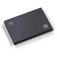
ispPAC-CLK5620AV-01TN100I Lattice, ispPAC-CLK5620AV-01TN100I Datasheet - Page 38

ispPAC-CLK5620AV-01TN100I
Manufacturer Part Number
ispPAC-CLK5620AV-01TN100I
Description
Clock Drivers & Distribution ISP 0 Dlay Clck Gen w/Unv Fan-Out Buf I
Manufacturer
Lattice
Datasheet
1.ISPPAC-CLK5610AV-01TN48I.pdf
(51 pages)
Specifications of ispPAC-CLK5620AV-01TN100I
Minimum Operating Temperature
0 C
Mounting Style
SMD/SMT
Maximum Operating Temperature
70 C
Package / Case
TQFP-100
Lead Free Status / RoHS Status
Lead free / RoHS Compliant
Available stocks
Company
Part Number
Manufacturer
Quantity
Price
Company:
Part Number:
ISPPAC-CLK5620AV-01TN100I
Manufacturer:
LATTICE
Quantity:
210
Company:
Part Number:
ISPPAC-CLK5620AV-01TN100I
Manufacturer:
Lattice Semiconductor Corporation
Quantity:
10 000
Lattice Semiconductor
Figure 1-32. TAP States
When the correct logic sequence is applied to the TMS and TCK inputs, the TAP will exit the Test-Logic-Reset state
and move to the desired state. The next state after Test-Logic-Reset is Run-Test/Idle. Until a data or instruction shift
is performed, no action will occur in Run-Test/Idle (steady state = idle). After Run-Test/Idle, either a data or instruc-
tion shift is performed. The states of the Data and Instruction Register blocks are identical to each other differing
only in their entry points. When either block is entered, the first action is a capture operation. For the Data Regis-
ters, the Capture-DR state is very simple: it captures (parallel loads) data onto the selected serial data path (previ-
ously chosen with the appropriate instruction). For the Instruction Register, the Capture-IR state will always load
the IDCODE instruction. It will always enable the ID Register for readout if no other instruction is loaded prior to a
Shift-DR operation. This, in conjunction with mandated bit codes, allows a “blind” interrogation of any device in a
compliant IEEE 1149.1 serial chain. From the Capture state, the TAP transitions to either the Shift or Exit1 state.
Normally the Shift state follows the Capture state so that test data or status information can be shifted out or new
data shifted in. Following the Shift state, the TAP either returns to the Run-Test/Idle state via the Exit1 and Update
states or enters the Pause state via Exit1. The Pause state is used to temporarily suspend the shifting of data
through either the Data or Instruction Register while an external operation is performed. From the Pause state,
shifting can resume by reentering the Shift state via the Exit2 state or be terminated by entering the Run-Test/Idle
state via the Exit2 and Update states. If the proper instruction is shifted in during a Shift-IR operation, the next entry
into Run-Test/Idle initiates the test mode (steady state = test). This is when the device is actually programmed,
erased or verified. All other instructions are executed in the Update state.
Test Instructions
Like data registers, the IEEE 1149.1 standard also mandates the inclusion of certain instructions. It outlines the
function of three required and six optional instructions. Any additional instructions are left exclusively for the manu-
facturer to determine. The instruction word length is not mandated other than to be a minimum of two bits, with only
the BYPASS and EXTEST instruction code patterns being specifically called out (all ones and all zeroes respec-
tively). The ispClock5600A contains the required minimum instruction set as well as one from the optional instruc-
tion set. In addition, there are several proprietary instructions that allow the device to be configured and verified.
0
1
Test-Logic-Rst
Run-Test/Idle
Note: The value shown adjacent to each state transition in this figure
represents the signal present at TMS at the time of a rising edge at TCK.
0
1
1
0
Select-DR-Scan
1
Capture-DR
Update-DR
Pause-DR
Exit1-DR
Exit2-DR
Shift-DR
1-38
0
0
1
0
1
1
0
1
1
0
0
ispClock5600A Family Data Sheet
1
0
Select-IR-Scan
1
Capture-IR
Update-IR
Pause-IR
Exit1-IR
Exit2-IR
Shift-IR
0
0
1
0
1
1
0
1
1
0
0


