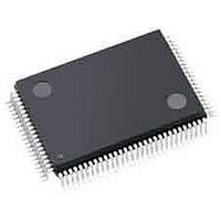
ispPAC-CLK5620AV-01TN100I Lattice, ispPAC-CLK5620AV-01TN100I Datasheet - Page 2

ispPAC-CLK5620AV-01TN100I
Manufacturer Part Number
ispPAC-CLK5620AV-01TN100I
Description
Clock Drivers & Distribution ISP 0 Dlay Clck Gen w/Unv Fan-Out Buf I
Manufacturer
Lattice
Datasheet
1.ISPPAC-CLK5610AV-01TN48I.pdf
(51 pages)
Specifications of ispPAC-CLK5620AV-01TN100I
Minimum Operating Temperature
0 C
Mounting Style
SMD/SMT
Maximum Operating Temperature
70 C
Package / Case
TQFP-100
Lead Free Status / RoHS Status
Lead free / RoHS Compliant
Available stocks
Company
Part Number
Manufacturer
Quantity
Price
Company:
Part Number:
ISPPAC-CLK5620AV-01TN100I
Manufacturer:
LATTICE
Quantity:
210
Company:
Part Number:
ISPPAC-CLK5620AV-01TN100I
Manufacturer:
Lattice Semiconductor Corporation
Quantity:
10 000
Lattice Semiconductor
General Description and Overview
The ispClock5610A and ispClock5620A are in-system-programmable high-fanout enhanced zero delay clock gen-
erators designed for use in high performance communications and computing applications. The ispClock5610A
provides up to 10 single-ended or five differential clock outputs, while the ispClock5620A provides up to 20 single-
ended or 10 differential clock outputs. Each pair of outputs may be independently configured to support separate
I/O standards (LVDS, LVPECL, LVTTL, LVCMOS, SSTL, HSTL) and output frequency. In addition, each output
provides independent programmable control of termination, slew-rate, and timing skew. All configuration informa-
tion is stored on-chip in non-volatile E
The ispClock5600A’s PLL and divider systems supports the synthesis of multiple clock frequencies derived from
the reference input through the provision of programmable input and feedback dividers. A set of five post-PLL V-
dividers provides additional flexibility by supporting the generation of five separate output frequencies. Loop feed-
back may be taken internally from the output of any of the five V-dividers, or externally through FBKA+/- or FBKB+/-
pins.
The core functions of all members of the ispClock5600A family are identical, the differences between devices being
restricted to the number of inputs and outputs, as shown in the following table. Figures 1 and 2 show functional
block diagrams of the ispClock5610A and ispClock5620A.
Table 1-1. ispClock5600A Family Members
Figure 1-1. ispClock5610A Functional Block Diagram
REFVTT
FBKVTT
REFA+
FBKA+
FBKA -
REFA-
ispClock5610A
ispClock5620A
0
Profile Select
PS0
Device
Control
1
DIVIDER
INPUT
(1-40)
(1-40)
PS1
2
M
N
3
FEEDBACK
TDI
DIVIDER
E
2
JTAG INTERFACE
Configuration
TMS
DETECT
DETECT
PHASE
LOCK
LOCK
TCK
2
Ref. Input Pairs
CMOS memory.
TDO
FILTER
LOOP
1
2
RESET
VCO
1-2
PLL_BYPASS
Feedback Input Pairs
SKEW ADJUST
FEEDBACK
1
0
DIVIDERS
1
2
OUTPUT
(2-80)
(2-80)
(2-80)
(2-80)
(2-80)
V0
V1
V2
V3
V4
ispClock5600A Family Data Sheet
SGATE
OUTPUT ENABLE CONTROLS
OUTPUT ROUTING
GOE
MATRIX
OEX
Clock Outputs
OEY
CONTROL
10
20
SKEW
DRIVERS
OUTPUT
BANK_0
BANK_0
BANK_1
BANK_1
BANK_2
BANK_2
BANK_3
BANK_3
BANK_4
BANK_4


