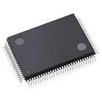
ispPAC-CLK5620AV-01TN100I Lattice, ispPAC-CLK5620AV-01TN100I Datasheet - Page 27

ispPAC-CLK5620AV-01TN100I
Manufacturer Part Number
ispPAC-CLK5620AV-01TN100I
Description
Clock Drivers & Distribution ISP 0 Dlay Clck Gen w/Unv Fan-Out Buf I
Manufacturer
Lattice
Datasheet
1.ISPPAC-CLK5610AV-01TN48I.pdf
(51 pages)
Specifications of ispPAC-CLK5620AV-01TN100I
Minimum Operating Temperature
0 C
Mounting Style
SMD/SMT
Maximum Operating Temperature
70 C
Package / Case
TQFP-100
Lead Free Status / RoHS Status
Lead free / RoHS Compliant
Available stocks
Company
Part Number
Manufacturer
Quantity
Price
Company:
Part Number:
ISPPAC-CLK5620AV-01TN100I
Manufacturer:
LATTICE
Quantity:
210
Company:
Part Number:
ISPPAC-CLK5620AV-01TN100I
Manufacturer:
Lattice Semiconductor Corporation
Quantity:
10 000
Lattice Semiconductor
Figure 1-22 shows a typical configuration for the ispClock5600A’s output driver when configured to drive SSTL2,
SSTL3, HSTL or eHSTL loads. The ispClock5600A’s output impedance should be set to 40Ω for driving SSTL2 or
SSTL3 loads and to the ≈20Ω setting for driving HSTL and eHSTL. The far end of the transmission line must be ter-
minated to an appropriate VTT voltage through a 50Ω resistor.
Figure 1-22. Configuration for SSTL2, SSTL3, and HSTL Output Modes
Figure 1-23 shows a typical configuration for the ispClock5600A’s output driver when configured to drive LVDS or
differential LVPECL loads. The ispClock5600A’s output impedance is disengaged when the driver is set to LVDS or
LVPECL mode. The far end of the transmission line must be terminated with a 100Ω resistor across the two signal
lines.
Figure 1-23. Configuration for LVDS and LVPECL Output Modes
Note that when in LVPECL output mode, the ispClock5600A’s output driver provides an internal pull-down, unlike a
typical bipolar LVPECL driver. For this reason no external pull-down resistors are necessary and the driver may be
terminated with a single 100Ω resistor across the signal lines. For proper operation, pull-down resistors should
NOT be used with the ispClock5600A’s LVPECL output mode.
Output Enable Controls
The ispClock5600A family provides the user with several options for enabling and disabling output pins, as well as
suspending the output clock. In addition to providing the user with the ability to reduce the device’s power con-
sumption by turning off unused drivers, these features can also be used for functional testing purposes. The follow-
ing input pins are used for output enable functions:
Additionally, internal E
external control pins.
• GOE – global output enable
• OEX, OEY – secondary output enable controls
• SGATE – synchronous output control
LVDS/LVPECL
Ro : 40 (SSTL)
SSTL/HSTL/eHSTL
mode
ispClock5600A
Mode
20 (HSTL, eHSTL)
2
CMOS configuration bits are provided for the purpose of modifying the effects of these
ispClock5600A
1-27
Zo=50
Zo=50
Zo=50
ispClock5600A Family Data Sheet
VREF
RT=50
VTT
RT=100
SSTL/HSTL/eHSTL
Receiver
LVDS/PECL
Receiver


