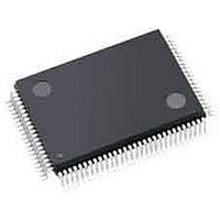
ispPAC-CLK5620AV-01TN100I Lattice, ispPAC-CLK5620AV-01TN100I Datasheet - Page 23

ispPAC-CLK5620AV-01TN100I
Manufacturer Part Number
ispPAC-CLK5620AV-01TN100I
Description
Clock Drivers & Distribution ISP 0 Dlay Clck Gen w/Unv Fan-Out Buf I
Manufacturer
Lattice
Datasheet
1.ISPPAC-CLK5610AV-01TN48I.pdf
(51 pages)
Specifications of ispPAC-CLK5620AV-01TN100I
Minimum Operating Temperature
0 C
Mounting Style
SMD/SMT
Maximum Operating Temperature
70 C
Package / Case
TQFP-100
Lead Free Status / RoHS Status
Lead free / RoHS Compliant
Available stocks
Company
Part Number
Manufacturer
Quantity
Price
Company:
Part Number:
ISPPAC-CLK5620AV-01TN100I
Manufacturer:
LATTICE
Quantity:
210
Company:
Part Number:
ISPPAC-CLK5620AV-01TN100I
Manufacturer:
Lattice Semiconductor Corporation
Quantity:
10 000
Lattice Semiconductor
ispClock5600A Family Data Sheet
LVDS/Differential LVPECL
The receiver should be set to LVDS or LVPECL mode as required and both termination resistors should be
engaged and set to 50Ω. The associated REFVTT or FBKVTT pin, however, should be left unconnected. This cre-
ates a floating 100Ω differential termination resistance across the input terminals. The LVDS termination configura-
tion is shown in Figure 1-18.
Figure 1-18. LVDS Input Receiver Configuration
ispClock5600A
Differential
+Signal In
Receiver
REFA+
LVDS
Driver
-Signal In
REFA-
50
50
CLOSED
CLOSED
No Connect
REFVTT
Note that while a floating 100Ω resistor forms a complete termination for an LVDS signal line, additional circuitry
may be required to satisfactorily terminate a differential LVPECL signal. This is because a true bipolar LVPECL out-
put driver typically requires an external DC ‘pull-down’ path to a V
termination voltage (typically VCC-2V) to
TERM
properly bias its open emitter output stage. When interfacing to an LVPECL input signal, the ispClock5600A’s inter-
nal termination resistors should not be used for this pull-down function, as they may be damaged from excessive
current. The pull-down should be implemented with external resistors placed close to the LVPECL driver (Figure 1-
19)
Figure 1-19. LVPECL Input Receiver Configuration
ispClock5600A
Differential
+Signal In
Receiver
REFA+
LVPECL
Driver
-Signal In
REFA-
R
R
50
50
PD
PD
CLOSED
CLOSED
V
No Connect
TERM
REFVTT
Please note that while the above discussions specify using 50Ω termination impedances, the actual impedance
required to properly terminate the transmission line and maintain good signal integrity may vary from this ideal. The
1-23


