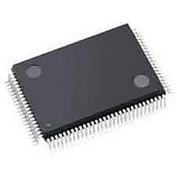
ispPAC-CLK5620AV-01TN100I Lattice, ispPAC-CLK5620AV-01TN100I Datasheet - Page 29

ispPAC-CLK5620AV-01TN100I
Manufacturer Part Number
ispPAC-CLK5620AV-01TN100I
Description
Clock Drivers & Distribution ISP 0 Dlay Clck Gen w/Unv Fan-Out Buf I
Manufacturer
Lattice
Datasheet
1.ISPPAC-CLK5610AV-01TN48I.pdf
(51 pages)
Specifications of ispPAC-CLK5620AV-01TN100I
Minimum Operating Temperature
0 C
Mounting Style
SMD/SMT
Maximum Operating Temperature
70 C
Package / Case
TQFP-100
Lead Free Status / RoHS Status
Lead free / RoHS Compliant
Available stocks
Company
Part Number
Manufacturer
Quantity
Price
Company:
Part Number:
ISPPAC-CLK5620AV-01TN100I
Manufacturer:
LATTICE
Quantity:
210
Company:
Part Number:
ISPPAC-CLK5620AV-01TN100I
Manufacturer:
Lattice Semiconductor Corporation
Quantity:
10 000
Lattice Semiconductor
ispClock5600A Family Data Sheet
For fine skew mode,
For coarse skew mode,
1
1
(5)
=
=
TU
TU
8f
4f
vco
vco
When an output driver is programmed to support a differential output mode, a single skew setting is applied to both
the BANKxA+ and BANKxB- signals. When the output driver is configured to support a single-ended output stan-
dard, each of the two single-ended outputs may be assigned independent skews.
By using the internal feedback path, and programming a skew into the feedback skew control, it is possible to
implement negative timing skews, in which the clock edge of interest appears at the ispClock5600A’s output before
the corresponding edge is presented at the reference input. When the feedback skew unit is used in this way, the
resulting negative skew is added to whatever skew is specified for each output. For example, if the feedback skew
is set to 6TU, BANK1’s skew is 8TU and BANK2’s skew is 3TU, then BANK1’s effective output skew will be 2TU
(8TU-6TU), while BANK2’s effective skew will be -3TU (3TU-6TU). This negative skew will manifest itself as
BANK2’s outputs appearing to lead the input reference clock, appearing as a negative propagation delay.
Please note that the skew control units are only usable when the PLL is selected. In PLL bypass mode
(PLL_BYPASS=1), output skew settings will be ineffective and all outputs will exhibit skew consistent with the
device’s propagation delay and the individual delays inherent in the output drivers consistent with the logic stan-
dard selected.
Coarse Skew Mode
The ispClock5600A family provides the user with the option of obtaining longer skew delays at the cost of reduced
time resolution through the use of coarse skew mode. Coarse skew mode provides unit delays ranging from 312ps
(f
= 800MHz) to 780ps (f
= 320MHz), which is twice as long as those provided in fine skew mode. When
VCO
VCO
coarse skew mode is selected, an additional divide-by-2 stage is effectively inserted between the VCO and the V-
divider bank, as shown in Figure 1-24. When assigning divider settings in coarse skew mode, one must account for
this additional divide-by-two so that the VCO still operates within its specified range (320-800MHz).
Figure 1-24. Additional Factor-of-2 Division in Coarse Mode
Fine
Mode
VCO
V-dividers
Fout
Coarse
Mode
÷2
When one moves from fine skew mode to coarse skew mode with a giveN-Divider configuration, the VCO fre-
quency will attempt to double to compensate for the additional divide-by-2 stage. Because the f
range is not
VCO
increased, however, one must modify the feedback path V-divider settings to bring f
back into its specified oper-
VCO
ating range (320MHz to 800MHz). This can be accomplished by dividing all V-divider settings by two. All output fre-
quencies will remain unchanged from what they were in fine mode. One drawback of moving from fine skew mode
into coarse skew mode is that it may not be possible to maintain consistent output frequencies, as only those V-
divider settings which are multiples of four (in fine mode) may be divided by two. For example, a V-divider setting of
24 will divide down to 12, which is also a legal V-divider setting, whereas an initial setting of 26 would divide down
to 13, which is not a valid setting.
When one moves from coarse skew mode to fine skew mode, the extra divide-by-two factor is removed from
between the VCO and the V-divider bank, halving the VCO’s effective operating frequency. To compensate for this
change, all of the V-dividers must be doubled to move the VCO back into its specified operating range and maintain
consistent output frequencies. The only situation in which this may be a problem is when a V-divider initially in
1-29


