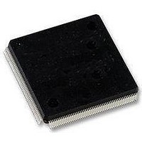
LFXP2-5E-5QN208C Lattice, LFXP2-5E-5QN208C Datasheet - Page 13

LFXP2-5E-5QN208C
Manufacturer Part Number
LFXP2-5E-5QN208C
Description
FPGA - Field Programmable Gate Array 5K LUTs 146I/O Inst- on DSP 1.2V -5 Spd
Manufacturer
Lattice
Datasheet
1.LFXP2-40E-5FN484I.pdf
(92 pages)
Specifications of LFXP2-5E-5QN208C
Number Of Macrocells
5000
Maximum Operating Frequency
200 MHz
Number Of Programmable I/os
146
Data Ram Size
10 KB
Supply Voltage (max)
1.14 V
Supply Current
17 mA
Maximum Operating Temperature
+ 85 C
Minimum Operating Temperature
0 C
Mounting Style
SMD/SMT
Supply Voltage (min)
1.26 V
Package / Case
PQFP-208
Lead Free Status / RoHS Status
Lead free / RoHS Compliant
Available stocks
Company
Part Number
Manufacturer
Quantity
Price
Company:
Part Number:
LFXP2-5E-5QN208C
Manufacturer:
Lattice Semiconductor Corporation
Quantity:
10 000
Part Number:
LFXP2-5E-5QN208C
Manufacturer:
LATTICE
Quantity:
20 000
Lattice Semiconductor
Secondary Clock/Control Sources
LatticeXP2 devices derive secondary clocks (SC0 through SC7) from eight dedicated clock input pads and the rest
from routing. Figure 2-7 shows the secondary clock sources.
Figure 2-7. Secondary Clock Sources
Clock Input
Clock Input
From Routing
From Routing
From Routing
From Routing
Routing
Routing
From
From
Routing
Routing
From
From
Secondary Clock Sources
Clock
Clock
Input
Input
2-10
Clock
Clock
Input
Input
Routing
Routing
From
From
LatticeXP2 Family Data Sheet
Routing
Routing
From
From
From Routing
From Routing
From Routing
From Routing
Clock Input
Clock Input
Architecture


