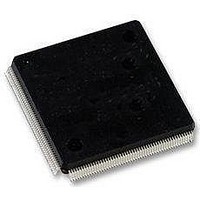
LFXP2-5E-5QN208C Lattice, LFXP2-5E-5QN208C Datasheet - Page 82

LFXP2-5E-5QN208C
Manufacturer Part Number
LFXP2-5E-5QN208C
Description
FPGA - Field Programmable Gate Array 5K LUTs 146I/O Inst- on DSP 1.2V -5 Spd
Manufacturer
Lattice
Datasheet
1.LFXP2-40E-5FN484I.pdf
(92 pages)
Specifications of LFXP2-5E-5QN208C
Number Of Macrocells
5000
Maximum Operating Frequency
200 MHz
Number Of Programmable I/os
146
Data Ram Size
10 KB
Supply Voltage (max)
1.14 V
Supply Current
17 mA
Maximum Operating Temperature
+ 85 C
Minimum Operating Temperature
0 C
Mounting Style
SMD/SMT
Supply Voltage (min)
1.26 V
Package / Case
PQFP-208
Lead Free Status / RoHS Status
Lead free / RoHS Compliant
Available stocks
Company
Part Number
Manufacturer
Quantity
Price
Company:
Part Number:
LFXP2-5E-5QN208C
Manufacturer:
Lattice Semiconductor Corporation
Quantity:
10 000
Part Number:
LFXP2-5E-5QN208C
Manufacturer:
LATTICE
Quantity:
20 000
Pin Information Summary (Cont.)
Lattice Semiconductor
Logic Signal Connections
Package pinout information can be found under “Data Sheets” on the LatticeXP2 product page of the Lattice web-
site a www.latticesemi.com/products/fpga/xp2 and in the Lattice ispLEVER software.
Thermal Management
Thermal management is recommended as part of any sound FPGA design methodology. To assess the thermal
characteristics of a system, Lattice specifies a maximum allowable junction temperature in all device data sheets.
Designers must complete a thermal analysis of their specific design to ensure that the device and package do not
exceed the junction temperature limits. Refer to the Lattice
package specific thermal values.
For Further Information
• TN1139,
• Power Calculator tool included with Lattice’s ispLEVER design tool, or as a standalone download from
PCI capable I/Os
Bonding Out per
Bank
1. Minimum requirement to implement a fully functional 8-bit wide DDR bus. Available DDR interface consists of at least 12 I/Os (1 DQS + 1 DQSB + 8 DQs + 1 DM
www.latticesemi.com/products/designsoftware
+ Bank VREF1).
Pin Type
Power Estimation and Management for LatticeXP2 Devices
Bank0
Bank1
Bank2
Bank3
Bank4
Bank5
Bank6
Bank7
csBGA
132
18
14
4
0
0
8
0
0
TQFP
144
20
18
6
0
0
8
0
0
XP2-5
PQFP
208
20
18
18
20
0
0
0
0
ftBGA
256
26
18
18
24
0
0
0
0
csBGA
132
18
14
4
0
0
8
0
0
TQFP
144
20
18
6
0
0
8
0
0
XP2-8
4-5
PQFP
208
20
18
18
20
0
0
0
0
Thermal Management
ftBGA
256
28
22
26
24
0
0
0
0
PQFP
208
20
18
18
20
0
0
0
0
XP2-17
ftBGA
256
28
22
26
24
0
0
0
0
LatticeXP2 Family Data Sheet
fpBGA
484
52
36
36
52
0
0
0
0
ftBGA
document to find the device/
256
28
22
26
24
0
0
0
0
Pinout Information
XP2-30
fpBGA
484
52
36
38
53
0
0
0
0
fpBGA
672
70
54
54
70
0
0
0
0
fpBGA
484
52
36
38
53
0
0
0
0
XP2-40
fpBGA
672
70
70
70
70
0
0
0
0


