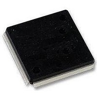
LFXP2-5E-5QN208C Lattice, LFXP2-5E-5QN208C Datasheet - Page 64

LFXP2-5E-5QN208C
Manufacturer Part Number
LFXP2-5E-5QN208C
Description
FPGA - Field Programmable Gate Array 5K LUTs 146I/O Inst- on DSP 1.2V -5 Spd
Manufacturer
Lattice
Datasheet
1.LFXP2-40E-5FN484I.pdf
(92 pages)
Specifications of LFXP2-5E-5QN208C
Number Of Macrocells
5000
Maximum Operating Frequency
200 MHz
Number Of Programmable I/os
146
Data Ram Size
10 KB
Supply Voltage (max)
1.14 V
Supply Current
17 mA
Maximum Operating Temperature
+ 85 C
Minimum Operating Temperature
0 C
Mounting Style
SMD/SMT
Supply Voltage (min)
1.26 V
Package / Case
PQFP-208
Lead Free Status / RoHS Status
Lead free / RoHS Compliant
Available stocks
Company
Part Number
Manufacturer
Quantity
Price
Company:
Part Number:
LFXP2-5E-5QN208C
Manufacturer:
Lattice Semiconductor Corporation
Quantity:
10 000
Part Number:
LFXP2-5E-5QN208C
Manufacturer:
LATTICE
Quantity:
20 000
Lattice Semiconductor
LatticeXP2 Internal Switching Characteristics
t
t
EBR Timing
t
t
t
t
t
t
t
t
t
t
t
t
t
t
t
PLL Parameters
t
t
DSP Block Timing
t
t
t
RST_PIO
DEL
CO_EBR
COO_EBR
SUDATA_EBR
HDATA_EBR
SUADDR_EBR
HADDR_EBR
SUWREN_EBR
HWREN_EBR
SUCE_EBR
HCE_EBR
RSTO_EBR
SUBE_EBR
HBE_EBR
RSTREC_EBR
RST_EBR
RSTKREC_PLL
RSTREC_PLL
SUI_DSP
HI_DSP
SUP_DSP
Parameter
Asynchronous reset time for PFU
Logic
Dynamic Delay Step Size
Clock (Read) to Output from
Address or Data
Clock (Write) to Output from EBR
Output Register
Setup Data to EBR Memory
(Write Clk)
Hold Data to EBR Memory (Write
Clk)
Setup Address to EBR Memory
(Write Clk)
Hold Address to EBR Memory
(Write Clk)
Setup Write/Read Enable to EBR
Memory (Write/Read Clk)
Hold Write/Read Enable to EBR
Memory (Write/Read Clk)
Clock Enable Setup Time to EBR
Output Register (Read Clk)
Clock Enable Hold Time to EBR
Output Register (Read Clk)
Reset To Output Delay Time from
EBR Output Register (Asynchro-
nous)
Byte Enable Set-Up Time to EBR
Output Register
Byte Enable Hold Time to EBR
Output Register Dynamic Delay
on Each PIO
Asynchronous reset recovery
time for EBR
Asynchronous reset time for EBR
After RSTK De-assert, Recovery
Time Before Next Clock Edge
Can Toggle K-divider Counter
After RST De-assert, Recovery
Time Before Next Clock Edge
Can Toggle M-divider Counter
(Applies to M-Divider Portion of
RST Only
Input Register Setup Time
Input Register Hold Time
Pipeline Register Setup Time
2
)
Description
Over Recommended Operating Conditions
-0.167
-0.117
-0.135
-0.097
-0.117
0.035
0.194
0.157
0.158
0.144
0.157
0.233
1.000
1.000
0.135
0.021
2.505
Min.
—
—
—
—
—
-7
3-20
0.386
0.035
2.774
0.360
1.156
1.156
Max.
—
—
—
—
—
—
—
—
—
—
—
—
—
—
—
—
-0.198
-0.137
-0.159
-0.113
-0.137
-0.006
0.035
0.231
0.182
0.186
0.160
0.182
0.291
1.000
1.000
0.151
2.784
Min.
1
—
—
—
—
—
(Continued)
DC and Switching Characteristics
-6
LatticeXP2 Family Data Sheet
0.419
0.035
3.142
0.408
1.341
1.341
Max.
—
—
—
—
—
—
—
—
—
—
—
—
—
—
—
—
-0.229
-0.157
-0.182
-0.129
-0.157
-0.031
0.035
0.267
0.207
0.214
0.176
0.207
0.347
1.000
1.000
0.166
3.064
Min.
—
—
—
—
—
-5
0.452
0.035
3.510
0.456
1.526
1.526
Max.
—
—
—
—
—
—
—
—
—
—
—
—
—
—
—
—
Units
ns
ns
ns
ns
ns
ns
ns
ns
ns
ns
ns
ns
ns
ns
ns
ns
ns
ns
ns
ns
ns
ns


