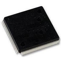
LFXP2-5E-5QN208C Lattice, LFXP2-5E-5QN208C Datasheet - Page 4

LFXP2-5E-5QN208C
Manufacturer Part Number
LFXP2-5E-5QN208C
Description
FPGA - Field Programmable Gate Array 5K LUTs 146I/O Inst- on DSP 1.2V -5 Spd
Manufacturer
Lattice
Datasheet
1.LFXP2-40E-5FN484I.pdf
(92 pages)
Specifications of LFXP2-5E-5QN208C
Number Of Macrocells
5000
Maximum Operating Frequency
200 MHz
Number Of Programmable I/os
146
Data Ram Size
10 KB
Supply Voltage (max)
1.14 V
Supply Current
17 mA
Maximum Operating Temperature
+ 85 C
Minimum Operating Temperature
0 C
Mounting Style
SMD/SMT
Supply Voltage (min)
1.26 V
Package / Case
PQFP-208
Lead Free Status / RoHS Status
Lead free / RoHS Compliant
Available stocks
Company
Part Number
Manufacturer
Quantity
Price
Company:
Part Number:
LFXP2-5E-5QN208C
Manufacturer:
Lattice Semiconductor Corporation
Quantity:
10 000
Part Number:
LFXP2-5E-5QN208C
Manufacturer:
LATTICE
Quantity:
20 000
LatticeXP2 Family Data Sheet
Architecture
August 2008
Data Sheet DS1009
Architecture Overview
Each LatticeXP2 device contains an array of logic blocks surrounded by Programmable I/O Cells (PIC). Inter-
spersed between the rows of logic blocks are rows of sysMEM™ Embedded Block RAM (EBR) and a row of sys-
DSP™ Digital Signal Processing blocks as shown in Figure 2-1.
On the left and right sides of the Programmable Functional Unit (PFU) array, there are Non-volatile Memory Blocks.
In configuration mode the nonvolatile memory is programmed via the IEEE 1149.1 TAP port or the sysCONFIG™
peripheral port. On power up, the configuration data is transferred from the Non-volatile Memory Blocks to the con-
figuration SRAM. With this technology, expensive external configuration memory is not required, and designs are
secured from unauthorized read-back. This transfer of data from non-volatile memory to configuration SRAM via
wide busses happens in microseconds, providing an “instant-on” capability that allows easy interfacing in many
applications. LatticeXP2 devices can also transfer data from the sysMEM EBR blocks to the Non-volatile Memory
Blocks at user request.
There are two kinds of logic blocks, the PFU and the PFU without RAM (PFF). The PFU contains the building
blocks for logic, arithmetic, RAM and ROM functions. The PFF block contains building blocks for logic, arithmetic
and ROM functions. Both PFU and PFF blocks are optimized for flexibility allowing complex designs to be imple-
mented quickly and efficiently. Logic Blocks are arranged in a two-dimensional array. Only one type of block is used
per row.
LatticeXP2 devices contain one or more rows of sysMEM EBR blocks. sysMEM EBRs are large dedicated 18Kbit
memory blocks. Each sysMEM block can be configured in a variety of depths and widths of RAM or ROM. In addi-
tion, LatticeXP2 devices contain up to two rows of DSP Blocks. Each DSP block has multipliers and adder/accumu-
lators, which are the building blocks for complex signal processing capabilities.
Each PIC block encompasses two PIOs (PIO pairs) with their respective sysIO buffers. The sysIO buffers of the
LatticeXP2 devices are arranged into eight banks, allowing the implementation of a wide variety of I/O standards.
PIO pairs on the left and right edges of the device can be configured as LVDS transmit/receive pairs. The PIC logic
also includes pre-engineered support to aid in the implementation of high speed source synchronous standards
such as 7:1 LVDS interfaces, found in many display applications, and memory interfaces including DDR and DDR2.
Other blocks provided include PLLs and configuration functions. The LatticeXP2 architecture provides up to four
General Purpose PLLs (GPLL) per device. The GPLL blocks are located in the corners of the device.
The configuration block that supports features such as configuration bit-stream de-encryption, transparent updates
and dual boot support is located between banks two and three. Every device in the LatticeXP2 family supports a
sysCONFIG port, muxed with bank seven I/Os, which supports serial device configuration. A JTAG port is provided
between banks two and three.
This family also provides an on-chip oscillator and Soft Error Detect (SED) capability. LatticeXP2 devices use 1.2V
as their core voltage.
© 2008 Lattice Semiconductor Corp. All Lattice trademarks, registered trademarks, patents, and disclaimers are as listed at www.latticesemi.com/legal. All other brand
or product names are trademarks or registered trademarks of their respective holders. The specifications and information herein are subject to change without notice.
www.latticesemi.com
2-1
DS1009
Architecture_01.4


