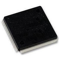
LFXP2-5E-5QN208C Lattice, LFXP2-5E-5QN208C Datasheet - Page 30

LFXP2-5E-5QN208C
Manufacturer Part Number
LFXP2-5E-5QN208C
Description
FPGA - Field Programmable Gate Array 5K LUTs 146I/O Inst- on DSP 1.2V -5 Spd
Manufacturer
Lattice
Datasheet
1.LFXP2-40E-5FN484I.pdf
(92 pages)
Specifications of LFXP2-5E-5QN208C
Number Of Macrocells
5000
Maximum Operating Frequency
200 MHz
Number Of Programmable I/os
146
Data Ram Size
10 KB
Supply Voltage (max)
1.14 V
Supply Current
17 mA
Maximum Operating Temperature
+ 85 C
Minimum Operating Temperature
0 C
Mounting Style
SMD/SMT
Supply Voltage (min)
1.26 V
Package / Case
PQFP-208
Lead Free Status / RoHS Status
Lead free / RoHS Compliant
Available stocks
Company
Part Number
Manufacturer
Quantity
Price
Company:
Part Number:
LFXP2-5E-5QN208C
Manufacturer:
Lattice Semiconductor Corporation
Quantity:
10 000
Part Number:
LFXP2-5E-5QN208C
Manufacturer:
LATTICE
Quantity:
20 000
Lattice Semiconductor
Table 2-11. PIO Signal List
PIO
The PIO contains four blocks: an input register block, output register block, tristate register block and a control logic
block. These blocks contain registers for operating in a variety of modes along with necessary clock and selection
logic.
Input Register Block
The input register blocks for PIOs contain delay elements and registers that can be used to condition high-speed
interface signals, such as DDR memory interfaces and source synchronous interfaces, before they are passed to
the device core. Figure 2-26 shows the diagram of the input register block.
Input signals are fed from the sysIO buffer to the input register block (as signal DI). If desired, the input signal can
bypass the register and delay elements and be used directly as a combinatorial signal (INDD), a clock (INCK) and,
in selected blocks, the input to the DQS delay block. If an input delay is desired, designers can select either a fixed
delay or a dynamic delay DEL[3:0]. The delay, if selected, reduces input register hold time requirements when
using a global clock.
The input block allows three modes of operation. In the Single Data Rate (SDR) mode, the data is registered, by
one of the registers in the SDR Sync register block, with the system clock. In DDR mode two registers are used to
sample the data on the positive and negative edges of the DQS signal which creates two data streams, D0 and D2.
D0 and D2 are synchronized with the system clock before entering the core. Further information on this topic can
be found in the DDR Memory Support section of this data sheet.
By combining input blocks of the complementary PIOs and sharing registers from output blocks, a gearbox function
can be implemented, that takes a double data rate signal applied to PIOA and converts it as four data streams,
IPOS0A, IPOS1A, IPOS0B and IPOS1B. Figure 2-26 shows the diagram using this gearbox function. For more
information on this topic, please see TN1138,
CE
CLK
ECLK1, ECLK2
LSR
GSRN
INCK
DQS
INDD
INFF
IPOS0, IPOS1
QPOS0
QNEG0
OPOS0, ONEG0,
OPOS2, ONEG2
OPOS1 ONEG1
DEL[3:0]
TD
DDRCLKPOL
DQSXFER
1. Signals available on left/right/bottom only.
2. Selected I/O.
2
Name
1
1
, QPOS1
, QNEG1
1
1
Control from the core
Control from the core
Control from the core
Control from the core
Control from routing
Input to the core
Input to PIO
Input to the core
Input to the core
Input to the core
Input to the core
Input to the core
Output data from the core
Tristate control from the core
Control from the core
Tristate control from the core
Control from clock polarity bus Controls the polarity of the clock (CLK0) that feed the DDR input block
Control from core
Type
LatticeXP2 High Speed I/O
Clock enables for input and output block flip-flops
System clocks for input and output blocks
Fast edge clocks
Local Set/Reset
Global Set/Reset (active low)
Input to Primary Clock Network or PLL reference inputs
DQS signal from logic (routing) to PIO
Unregistered data input to core
Registered input on positive edge of the clock (CLK0)
Double data rate registered inputs to the core
Gearbox pipelined inputs to the core
Gearbox pipelined inputs to the core
Output signals from the core for SDR and DDR operation
Signals to Tristate Register block for DDR operation
Dynamic input delay control bits
Tristate signal from the core used in SDR operation
Controls signal to the Output block
2-27
Interface.
Description
LatticeXP2 Family Data Sheet
Architecture


