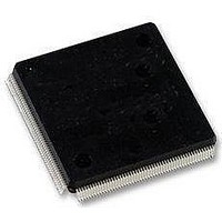
LFXP2-5E-5QN208C Lattice, LFXP2-5E-5QN208C Datasheet - Page 19

LFXP2-5E-5QN208C
Manufacturer Part Number
LFXP2-5E-5QN208C
Description
FPGA - Field Programmable Gate Array 5K LUTs 146I/O Inst- on DSP 1.2V -5 Spd
Manufacturer
Lattice
Datasheet
1.LFXP2-40E-5FN484I.pdf
(92 pages)
Specifications of LFXP2-5E-5QN208C
Number Of Macrocells
5000
Maximum Operating Frequency
200 MHz
Number Of Programmable I/os
146
Data Ram Size
10 KB
Supply Voltage (max)
1.14 V
Supply Current
17 mA
Maximum Operating Temperature
+ 85 C
Minimum Operating Temperature
0 C
Mounting Style
SMD/SMT
Supply Voltage (min)
1.26 V
Package / Case
PQFP-208
Lead Free Status / RoHS Status
Lead free / RoHS Compliant
Available stocks
Company
Part Number
Manufacturer
Quantity
Price
Company:
Part Number:
LFXP2-5E-5QN208C
Manufacturer:
Lattice Semiconductor Corporation
Quantity:
10 000
Part Number:
LFXP2-5E-5QN208C
Manufacturer:
LATTICE
Quantity:
20 000
Lattice Semiconductor
sysMEM Memory
LatticeXP2 devices contains a number of sysMEM Embedded Block RAM (EBR). The EBR consists of 18 Kbit
RAM with dedicated input and output registers.
sysMEM Memory Block
The sysMEM block can implement single port, dual port or pseudo dual port memories. Each block can be used in
a variety of depths and widths as shown in Table 2-5. FIFOs can be implemented in sysMEM EBR blocks by using
support logic with PFUs. The EBR block supports an optional parity bit for each data byte to facilitate parity check-
ing. EBR blocks provide byte-enable support for configurations with18-bit and 36-bit data widths.
Table 2-5. sysMEM Block Configurations
Bus Size Matching
All of the multi-port memory modes support different widths on each of the ports. The RAM bits are mapped LSB
word 0 to MSB word 0, LSB word 1 to MSB word 1, and so on. Although the word size and number of words for
each port varies, this mapping scheme applies to each port.
FlashBAK EBR Content Storage
All the EBR memory in the LatticeXP2 is shadowed by Flash memory. Optionally, initialization values for the mem-
ory blocks can be defined using the Lattice ispLEVER tools. The initialization values are loaded into the Flash
memory during device programming and into the SRAM at power up or whenever the device is reconfigured. This
feature is ideal for the storage of a variety of information such as look-up tables and microprocessor code. It is also
possible to write the current contents of the EBR memory back to Flash memory. This capability is useful for the
storage of data such as error codes and calibration information. For additional information on the FlashBAK capa-
bility see TN1137,
LatticeXP2 Memory Usage
Single Port
True Dual Port
Pseudo Dual Port
Memory Mode
Guide.
2-16
Configurations
16,384 x 1
1,024 x 18
16,384 x 1
1,024 x 18
16,384 x 1
1,024 x 18
8,192 x 2
4,096 x 4
2,048 x 9
8,192 x 2
4,096 x 4
2,048 x 9
8,192 x 2
4,096 x 4
2,048 x 9
512 x 36
512 x 36
LatticeXP2 Family Data Sheet
Architecture


