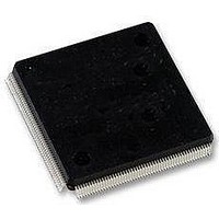
LFXP2-5E-5QN208C Lattice, LFXP2-5E-5QN208C Datasheet - Page 9

LFXP2-5E-5QN208C
Manufacturer Part Number
LFXP2-5E-5QN208C
Description
FPGA - Field Programmable Gate Array 5K LUTs 146I/O Inst- on DSP 1.2V -5 Spd
Manufacturer
Lattice
Datasheet
1.LFXP2-40E-5FN484I.pdf
(92 pages)
Specifications of LFXP2-5E-5QN208C
Number Of Macrocells
5000
Maximum Operating Frequency
200 MHz
Number Of Programmable I/os
146
Data Ram Size
10 KB
Supply Voltage (max)
1.14 V
Supply Current
17 mA
Maximum Operating Temperature
+ 85 C
Minimum Operating Temperature
0 C
Mounting Style
SMD/SMT
Supply Voltage (min)
1.26 V
Package / Case
PQFP-208
Lead Free Status / RoHS Status
Lead free / RoHS Compliant
Available stocks
Company
Part Number
Manufacturer
Quantity
Price
Company:
Part Number:
LFXP2-5E-5QN208C
Manufacturer:
Lattice Semiconductor Corporation
Quantity:
10 000
Part Number:
LFXP2-5E-5QN208C
Manufacturer:
LATTICE
Quantity:
20 000
Architecture
Lattice Semiconductor
LatticeXP2 Family Data Sheet
Routing
There are many resources provided in the LatticeXP2 devices to route signals individually or as busses with related
control signals. The routing resources consist of switching circuitry, buffers and metal interconnect (routing) seg-
ments.
The inter-PFU connections are made with x1 (spans two PFU), x2 (spans three PFU) or x6 (spans seven PFU)
connections. The x1 and x2 connections provide fast and efficient connections in horizontal and vertical directions.
The x2 and x6 resources are buffered to allow both short and long connections routing between PFUs.
The LatticeXP2 family has an enhanced routing architecture to produce a compact design. The ispLEVER design
tool takes the output of the synthesis tool and places and routes the design. Generally, the place and route tool is
completely automatic, although an interactive routing editor is available to optimize the design.
sysCLOCK Phase Locked Loops (PLL)
The sysCLOCK PLLs provide the ability to synthesize clock frequencies. The LatticeXP2 family supports between
two and four full featured General Purpose PLLs (GPLL). The architecture of the GPLL is shown in Figure 2-4.
CLKI, the PLL reference frequency, is provided either from the pin or from routing; it feeds into the Input Clock
Divider block. CLKFB, the feedback signal, is generated from CLKOP (the primary clock output) or from a user
clock pin/logic. CLKFB feeds into the Feedback Divider and is used to multiply the reference frequency.
Both the input path and feedback signals enter the Voltage Controlled Oscillator (VCO) block. The phase and fre-
quency of the VCO are determined from the input path and feedback signals. A LOCK signal is generated by the
VCO to indicate that the VCO is locked with the input clock signal.
The output of the VCO feeds into the CLKOP Divider, a post-scalar divider. The duty cycle of the CLKOP Divider
output can be fine tuned using the Duty Trim block, which creates the CLKOP signal. By allowing the VCO to oper-
ate at higher frequencies than CLKOP, the frequency range of the GPLL is expanded. The output of the CLKOP
Divider is passed through the CLKOK Divider, a secondary clock divider, to generate lower frequencies for the
CLKOK output. For applications that require even lower frequencies, the CLKOP signal is passed through a divide-
by-three divider to produce the CLKOK2 output. The CLKOK2 output is provided for applications that use source
synchronous logic. The Phase/Duty Cycle/Duty Trim block is used to adjust the phase and duty cycle of the CLKOP
Divider output to generate the CLKOS signal. The phase/duty cycle setting can be pre-programmed or dynamically
adjusted.
The clock outputs from the GPLL; CLKOP, CLKOK, CLKOK2 and CLKOS, are fed to the clock distribution network.
For further information on the GPLL please see TN1126,
LatticeXP2 sysCLOCK PLL Design and Usage
Guide.
2-6


