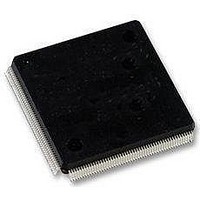
LFXP2-5E-5QN208C Lattice, LFXP2-5E-5QN208C Datasheet - Page 78

LFXP2-5E-5QN208C
Manufacturer Part Number
LFXP2-5E-5QN208C
Description
FPGA - Field Programmable Gate Array 5K LUTs 146I/O Inst- on DSP 1.2V -5 Spd
Manufacturer
Lattice
Datasheet
1.LFXP2-40E-5FN484I.pdf
(92 pages)
Specifications of LFXP2-5E-5QN208C
Number Of Macrocells
5000
Maximum Operating Frequency
200 MHz
Number Of Programmable I/os
146
Data Ram Size
10 KB
Supply Voltage (max)
1.14 V
Supply Current
17 mA
Maximum Operating Temperature
+ 85 C
Minimum Operating Temperature
0 C
Mounting Style
SMD/SMT
Supply Voltage (min)
1.26 V
Package / Case
PQFP-208
Lead Free Status / RoHS Status
Lead free / RoHS Compliant
Available stocks
Company
Part Number
Manufacturer
Quantity
Price
Company:
Part Number:
LFXP2-5E-5QN208C
Manufacturer:
Lattice Semiconductor Corporation
Quantity:
10 000
Part Number:
LFXP2-5E-5QN208C
Manufacturer:
LATTICE
Quantity:
20 000
Signal Descriptions
June 2008
© 2008 Lattice Semiconductor Corp. All Lattice trademarks, registered trademarks, patents, and disclaimers are as listed at www.latticesemi.com/legal. All other brand
or product names are trademarks or registered trademarks of their respective holders. The specifications and information herein are subject to change without notice.
www.latticesemi.com
General Purpose
P[Edge] [Row/Column Number*]_[A/B]
GSRN
NC
GND
V
V
V
V
V
PLL and Clock Functions (Used as user programmable I/O pins when not in use for PLL or clock pins)
[LOC][num]_V
[LOC][num]_GPLL[T, C]_IN_A
[LOC][num]_GPLL[T, C]_FB_A
PCLK[T, C]_[n:0]_[3:0]
[LOC]DQS[num]
Test and Programming (Dedicated Pins)
TMS
TCK
TDI
CC
CCAUX
CCPLL
CCIOx
REF1_x
, V
REF2_x
Signal Name
CCPLL
I/O
I/O
—
—
—
—
—
—
—
—
I
I
I
I
I
I
I
I
[Edge] indicates the edge of the device on which the pad is located. Valid
edge designations are L (Left), B (Bottom), R (Right), T (Top).
[Row/Column Number] indicates the PFU row or the column of the device on
which the PIC exists. When Edge is T (Top) or B (Bottom), only need to spec-
ify Row Number. When Edge is L (Left) or R (Right), only need to specify Col-
umn Number.
[A/B] indicates the PIO within the PIC to which the pad is connected. Some of
these user-programmable pins are shared with special function pins. These
pins, when not used as special purpose pins, can be programmed as I/Os for
user logic. During configuration the user-programmable I/Os are tri-stated
with an internal pull-up resistor enabled. If any pin is not used (or not bonded
to a package pin), it is also tri-stated with an internal pull-up resistor enabled
after configuration.
Global RESET signal (active low). Any I/O pin can be GSRN.
No connect.
Ground. Dedicated pins.
Power supply pins for core logic. Dedicated pins.
Auxiliary power supply pin. This dedicated pin powers all the differential and
referenced input buffers.
PLL supply pins. csBGA, PQFP and TQFP packages only.
Dedicated power supply pins for I/O bank x.
Reference supply pins for I/O bank x. Pre-determined pins in each bank are
assigned as V
Power supply pin for PLL: LLC, LRC, URC, ULC, num = row from center.
General Purpose PLL (GPLL) input pads: LLC, LRC, URC, ULC, num = row
from center, T = true and C = complement, index A,B,C...at each side.
Optional feedback GPLL input pads: LLC, LRC, URC, ULC, num = row from
center, T = true and C = complement, index A,B,C...at each side.
Primary Clock pads, T = true and C = complement, n per side, indexed by
bank and 0,1,2,3 within bank.
DQS input pads: T (Top), R (Right), B (Bottom), L (Left), DQS, num = ball
function number. Any pad can be configured to be output.
Test Mode Select input, used to control the 1149.1 state machine. Pull-up is
enabled during configuration.
Test Clock input pin, used to clock the 1149.1 state machine. No pull-up
enabled.
Test Data in pin. Used to load data into device using 1149.1 state machine.
After power-up, this TAP port can be activated for configuration by sending
appropriate command. (Note: once a configuration port is selected it is
locked. Another configuration port cannot be selected until the power-up
sequence). Pull-up is enabled during configuration.
LatticeXP2 Family Data Sheet
4-1
REF
inputs. When not used, they may be used as I/O pins.
Description
Pinout Information
Pinout Information_01.5
Data Sheet DS1009


