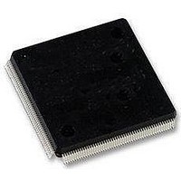
LFXP2-5E-5QN208C Lattice, LFXP2-5E-5QN208C Datasheet - Page 15

LFXP2-5E-5QN208C
Manufacturer Part Number
LFXP2-5E-5QN208C
Description
FPGA - Field Programmable Gate Array 5K LUTs 146I/O Inst- on DSP 1.2V -5 Spd
Manufacturer
Lattice
Datasheet
1.LFXP2-40E-5FN484I.pdf
(92 pages)
Specifications of LFXP2-5E-5QN208C
Number Of Macrocells
5000
Maximum Operating Frequency
200 MHz
Number Of Programmable I/os
146
Data Ram Size
10 KB
Supply Voltage (max)
1.14 V
Supply Current
17 mA
Maximum Operating Temperature
+ 85 C
Minimum Operating Temperature
0 C
Mounting Style
SMD/SMT
Supply Voltage (min)
1.26 V
Package / Case
PQFP-208
Lead Free Status / RoHS Status
Lead free / RoHS Compliant
Available stocks
Company
Part Number
Manufacturer
Quantity
Price
Company:
Part Number:
LFXP2-5E-5QN208C
Manufacturer:
Lattice Semiconductor Corporation
Quantity:
10 000
Part Number:
LFXP2-5E-5QN208C
Manufacturer:
LATTICE
Quantity:
20 000
Lattice Semiconductor
Primary Clock Routing
The clock routing structure in LatticeXP2 devices consists of a network of eight primary clock lines (CLK0 through
CLK7) per quadrant. The primary clocks of each quadrant are generated from muxes located in the center of the
device. All the clock sources are connected to these muxes. Figure 2-9 shows the clock routing for one quadrant.
Each quadrant mux is identical. If desired, any clock can be routed globally.
Figure 2-9. Per Quadrant Primary Clock Selection
Dynamic Clock Select (DCS)
The DCS is a smart multiplexer function available in the primary clock routing. It switches between two independent
input clock sources without any glitches or runt pulses. This is achieved irrespective of when the select signal is
toggled. There are two DCS blocks per quadrant; in total, eight DCS blocks per device. The inputs to the DCS block
come from the center muxes. The output of the DCS is connected to primary clocks CLK6 and CLK7 (see Figure 2-
9).
Figure 2-10 shows the timing waveforms of the default DCS operating mode. The DCS block can be programmed
to other modes. For more information on the DCS, please see TN1126,
Usage
Figure 2-10. DCS Waveforms
Secondary Clock/Control Routing
Secondary clocks in the LatticeXP2 devices are region-based resources. The benefit of region-based resources is
the relatively low injection delay and skew within the region, as compared to primary clocks. EBR rows, DSP rows
and a special vertical routing channel bound the secondary clock regions. This special vertical routing channel
aligns with either the left edge of the center DSP block in the DSP row or the center of the DSP row. Figure 2-11
shows this special vertical routing channel and the eight secondary clock regions for the LatticeXP2-40.
Guide.
CLK0
30:1
SEL
CLK1
CLK0
DCSOUT
CLK1
30:1
CLK2
Primary Clock Sources: PLLs + CLKDIVs + PIOs + Routing
30:1
8 Primary Clocks (CLK0 to CLK7) per Quadrant
CLK3
30:1
CLK4
30:1
2-12
CLK5
30:1
29:1
CLK6
DCS
LatticeXP2 sysCLOCK PLL Design and
LatticeXP2 Family Data Sheet
29:1
29:1
CLK7
DCS
29:1
Architecture


