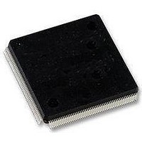
LFXP2-5E-5QN208C Lattice, LFXP2-5E-5QN208C Datasheet - Page 20

LFXP2-5E-5QN208C
Manufacturer Part Number
LFXP2-5E-5QN208C
Description
FPGA - Field Programmable Gate Array 5K LUTs 146I/O Inst- on DSP 1.2V -5 Spd
Manufacturer
Lattice
Datasheet
1.LFXP2-40E-5FN484I.pdf
(92 pages)
Specifications of LFXP2-5E-5QN208C
Number Of Macrocells
5000
Maximum Operating Frequency
200 MHz
Number Of Programmable I/os
146
Data Ram Size
10 KB
Supply Voltage (max)
1.14 V
Supply Current
17 mA
Maximum Operating Temperature
+ 85 C
Minimum Operating Temperature
0 C
Mounting Style
SMD/SMT
Supply Voltage (min)
1.26 V
Package / Case
PQFP-208
Lead Free Status / RoHS Status
Lead free / RoHS Compliant
Available stocks
Company
Part Number
Manufacturer
Quantity
Price
Company:
Part Number:
LFXP2-5E-5QN208C
Manufacturer:
Lattice Semiconductor Corporation
Quantity:
10 000
Part Number:
LFXP2-5E-5QN208C
Manufacturer:
LATTICE
Quantity:
20 000
Lattice Semiconductor
Figure 2-16. FlashBAK Technology
Memory Cascading
Larger and deeper blocks of RAMs can be created using EBR sysMEM Blocks. Typically, the Lattice design tools
cascade memory transparently, based on specific design inputs.
Single, Dual and Pseudo-Dual Port Modes
In all the sysMEM RAM modes the input data and address for the ports are registered at the input of the memory
array. The output data of the memory is optionally registered at the output.
EBR memory supports two forms of write behavior for single port or dual port operation:
1. Normal – Data on the output appears only during a read cycle. During a write cycle, the data (at the current
2. Write Through – A copy of the input data appears at the output of the same port during a write cycle. This
Memory Core Reset
The memory array in the EBR utilizes latches at the A and B output ports. These latches can be reset asynchro-
nously or synchronously. RSTA and RSTB are local signals, which reset the output latches associated with Port A
and Port B respectively. GSRN, the global reset signal, resets both ports. The output data latches and associated
resets for both ports are as shown in Figure 2-17.
Figure 2-17. Memory Core Reset
address) does not appear on the output. This mode is supported for all data widths.
mode is supported for all data widths.
FPGA Logic
GSRN
RSTA
RSTB
Make Infinite Reads and
Writes to EBR
Programmable Disable
EBR
Memory Core
2-17
Flash
Output Data
L
L
D
D
Latches
CLR
CLR
EBR During Configuration /
SET
SET
Write From EBR to Flash
Q
Q
Write to Flash During
Write From Flash to
on User Command
Programming
LatticeXP2 Family Data Sheet
JTAG / SPI Port
Port A[17:0]
Port B[17:0]
Architecture


