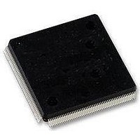
LFXP2-5E-5QN208C Lattice, LFXP2-5E-5QN208C Datasheet - Page 36

LFXP2-5E-5QN208C
Manufacturer Part Number
LFXP2-5E-5QN208C
Description
FPGA - Field Programmable Gate Array 5K LUTs 146I/O Inst- on DSP 1.2V -5 Spd
Manufacturer
Lattice
Datasheet
1.LFXP2-40E-5FN484I.pdf
(92 pages)
Specifications of LFXP2-5E-5QN208C
Number Of Macrocells
5000
Maximum Operating Frequency
200 MHz
Number Of Programmable I/os
146
Data Ram Size
10 KB
Supply Voltage (max)
1.14 V
Supply Current
17 mA
Maximum Operating Temperature
+ 85 C
Minimum Operating Temperature
0 C
Mounting Style
SMD/SMT
Supply Voltage (min)
1.26 V
Package / Case
PQFP-208
Lead Free Status / RoHS Status
Lead free / RoHS Compliant
Available stocks
Company
Part Number
Manufacturer
Quantity
Price
Company:
Part Number:
LFXP2-5E-5QN208C
Manufacturer:
Lattice Semiconductor Corporation
Quantity:
10 000
Part Number:
LFXP2-5E-5QN208C
Manufacturer:
LATTICE
Quantity:
20 000
Lattice Semiconductor
Figure 2-31. DQS Local Bus
Polarity Control Logic
In a typical DDR memory interface design, the phase relationship between the incoming delayed DQS strobe and
the internal system clock (during the READ cycle) is unknown. The LatticeXP2 family contains dedicated circuits to
transfer data between these domains. To prevent set-up and hold violations, at the domain transfer between DQS
(delayed) and the system clock, a clock polarity selector is used. This changes the edge on which the data is regis-
tered in the synchronizing registers in the input register block and requires evaluation at the start of each READ
cycle for the correct clock polarity.
Prior to the READ operation in DDR memories, DQS is in tristate (pulled by termination). The DDR memory device
drives DQS low at the start of the preamble state. A dedicated circuit detects this transition. This signal is used to
control the polarity of the clock to the synchronizing registers.
*DQSXFERDEL shifts ECLK1 by 90% and is not associated with a particular PIO.
DQSXFER
DQS
DQS
DCNTL[6:0]
ECLK1
DQSXFER
DCNTL[6:0]
CLK1
GSR
DQS
CEI
2-33
DQSXFERDEL*
Polarity Control
DQSDEL
Logic
PIO
PIO
To DDR
Register Block
Register Block
Reg.
Output
Input
Calibration bus
To Sync
from DLL
Reg.
LatticeXP2 Family Data Sheet
Buffer
Buffer
sysIO
sysIO
DI
DI
Strobe
Datain
DDR
DQS
PAD
PAD
Architecture


