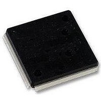
LFXP2-5E-5QN208C Lattice, LFXP2-5E-5QN208C Datasheet - Page 14

LFXP2-5E-5QN208C
Manufacturer Part Number
LFXP2-5E-5QN208C
Description
FPGA - Field Programmable Gate Array 5K LUTs 146I/O Inst- on DSP 1.2V -5 Spd
Manufacturer
Lattice
Datasheet
1.LFXP2-40E-5FN484I.pdf
(92 pages)
Specifications of LFXP2-5E-5QN208C
Number Of Macrocells
5000
Maximum Operating Frequency
200 MHz
Number Of Programmable I/os
146
Data Ram Size
10 KB
Supply Voltage (max)
1.14 V
Supply Current
17 mA
Maximum Operating Temperature
+ 85 C
Minimum Operating Temperature
0 C
Mounting Style
SMD/SMT
Supply Voltage (min)
1.26 V
Package / Case
PQFP-208
Lead Free Status / RoHS Status
Lead free / RoHS Compliant
Available stocks
Company
Part Number
Manufacturer
Quantity
Price
Company:
Part Number:
LFXP2-5E-5QN208C
Manufacturer:
Lattice Semiconductor Corporation
Quantity:
10 000
Part Number:
LFXP2-5E-5QN208C
Manufacturer:
LATTICE
Quantity:
20 000
Lattice Semiconductor
Edge Clock Sources
Edge clock resources can be driven from a variety of sources at the same edge. Edge clock resources can be
driven from adjacent edge clock PIOs, primary clock PIOs, PLLs and clock dividers as shown in Figure 2-8.
Figure 2-8. Edge Clock Sources
Note: This diagram shows sources for the XP2-17 device. Smaller LatticeXP2 devices have two GPLLs.
From Routing
From Routing
Sources for left edge clocks
Input
Input
PLL
PLL
Clock
Clock
Input
Input
GPLL
GPLL
CLKOP
CLKOS
CLKOP
CLKOS
Routing
Routing
From
From
Eight Edge Clocks (ECLK)
Two Clocks per Edge
Clock Input
Clock Input
2-11
Clock Input
Clock Input
Routing
Routing
From
From
Sources for top
bottom edge
Sources for
edge clocks
clocks
LatticeXP2 Family Data Sheet
Sources for right edge clocks
CLKOP
CLKOS GPLL
CLKOP
CLKOS GPLL
Architecture
From Routing
From Routing
Clock
Clock
Input
Input
Input
Input
PLL
PLL


